
High Speed Communication PCB: Reliable Design Solutions

Differential vs Single-Ended Signaling in High Speed Digital PCBs
- Noise immunity: Differential signaling provides 20–30 dB better common-mode rejection.
- Lower emissions: Complementary signals cancel radiated noise, easing compliance.
- Design tradeoffs: Differential pairs require careful length matching, increased routing density, and more layers.
For advanced designs like RF communication PCBs and communication circuit boards, the benefits of differential signaling outweigh the added complexity. Highleap Electronics supports customers with impedance modeling, pair routing optimization, and layer stackup guidance, ensuring signal integrity is preserved from prototype through mass production. Explore High Speed Communication PCB technologies with Highleap Electronics. Learn about high speed PCB design, signal integrity, via strategies, materials, and manufacturing solutions.
Copper Weight Selection in High Frequency PCBs
Copper thickness plays a critical role in both signal integrity and thermal performance. In high frequency PCBs, thinner copper such as 0.5 oz reduces skin effect losses, improving transmission quality at GHz frequencies. Thicker copper (2–4 oz) improves current capacity and heat spreading but introduces etching challenges for fine-pitch designs.
- Thin copper: Better high-frequency performance, easier impedance control.
- Thick copper: Improved thermal handling, higher current capacity, more manufacturing difficulty.
Smart strategies involve selective thickening — adding heavier copper only where heat or current demands justify it. At Highleap, our communication PCB assembly lines are equipped to manage boards with variable copper thickness, ensuring both fine signal routing and robust thermal management can coexist in a single design without compromising yield.
Via Technology for High Speed PCB Manufacturing
Via selection is a major factor in high speed PCB manufacturing. Through-hole vias are cost-effective but cause stub resonances at high frequencies. Blind and buried vias reduce signal path length and eliminate stubs, essential for high speed backplane PCBs and compact wireless devices.
- Through-hole vias: Economical but introduce resonances above 5 GHz.
- Blind vias: Connect surface to inner layers, minimizing discontinuities.
- Buried vias: Increase routing density while freeing surface space.
While advanced via options increase manufacturing complexity, they often unlock performance that standard designs cannot achieve. Highleap leverages sequential lamination, laser drilling, and back-drilling capabilities to deliver manufacturable solutions, helping customers balance performance gains with realistic production costs.

Stackup Strategies: Symmetric vs Asymmetric Configurations
Stackup design defines both mechanical stability and electrical behavior in high speed PCB design. Symmetric stackups ensure dimensional stability and simplify impedance modeling, while asymmetric stackups provide flexibility for routing and component placement.
- Symmetric stackups: Balanced copper distribution, reduced warpage, consistent impedance.
- Asymmetric stackups: Shorter via paths, more routing options, higher risk of warpage if not controlled.
Each approach has its place depending on size, frequency, and system requirements. Highleap works with customers during stackup planning to define the right configuration, ensuring manufacturability while meeting high-speed signal integrity goals. This expertise is particularly valuable for large-format communication PCBs, high speed backplane boards, and satellite communication modules where flatness and impedance stability are mission-critical.
Simulation Tools for Signal Integrity in High Speed Communication PCBs
Ensuring signal integrity requires both frequency domain and time domain simulations. Frequency domain analysis reveals resonances and frequency-dependent losses, while time domain analysis highlights eye diagrams, jitter, and crosstalk. Together, these tools allow engineers to verify high speed PCB design before prototyping.
Modern simulation platforms integrate both methods, providing comprehensive insights for mixed-signal designs. Highleap supports this process by correlating simulation results with real manufacturing tolerances and test coupon data, helping customers align theoretical performance with real-world outcomes. By combining advanced modeling with proven PCB fabrication workflows, we ensure that prototypes of RF boards, IoT modules, and other high speed communication systems behave as expected and can scale reliably to volume production.

Material Platforms: FR-4 vs Advanced Substrates
Material choice is a defining factor in high speed communication PCB performance. FR-4 remains the economical workhorse up to several GHz, but at higher frequencies, premium materials are required to ensure stable performance.
- FR-4: Cost-effective, widely available, suitable for moderate-speed designs.
- Rogers & Taconic: Low-loss laminates for multi-GHz and RF applications.
- Isola & Panasonic Megtron: Excellent stability and reliability at 10+ GHz data rates.
- Ceramic substrates (Al₂O₃, AlN): High thermal conductivity for power-intensive RF modules.
Hybrid stackups combining FR-4 with advanced laminates are increasingly popular, allowing cost-sensitive designs to leverage premium performance only where necessary. Highleap has extensive experience processing mixed-material boards, ensuring lamination compatibility, CTE matching, and reliable yields across both 5G communication PCBs and next-generation high-speed modules.
Conclusion: High Speed PCB Design with Reliable Manufacturing
Designing a high speed communication PCB involves complex tradeoffs across signaling, copper weight, vias, stackups, materials, and signal integrity validation. The lessons extend beyond communication boards to high frequency PCBs, high speed digital PCBs, and high speed backplane PCBs, all of which demand precision manufacturing and validation.
Highleap Electronics provides advanced high speed PCB manufacturing, precision impedance control, and hybrid stackup solutions. By combining signal integrity expertise with proven production capabilities, we ensure reliable outcomes for every signal integrity PCB. Contact our team to discuss how we can accelerate your next high speed communication PCB project with scalable and dependable manufacturing support.

Related Articles

How to Clean Flux Off a PCB: The Right Method for Each Flux Type
Figure 1. How To Clean Flux Off Pcb reference image for...
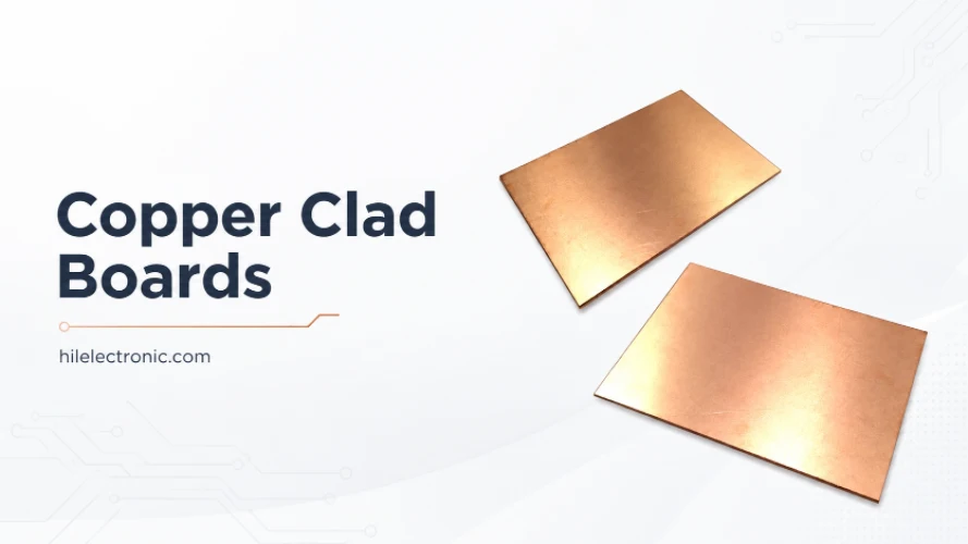
Copper Clad Boards (Copper-Clad Laminate): What They Are, Types, and How PCBs Are Made From Them
Figure 1. copper clad boards image for PCB manufacturing...
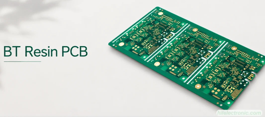
BT Resin PCB: Properties, Uses, and Fabrication Controls
Figure 1. BT resin PCB image for PCB manufacturing...
PCB Potting Services: Compounds, Process, and Design Rules
Figure 1. PCB potting services image for Highleap...
How to get a quote for PCBs
Let us run DFM/DFA analysis for you and get back to you with a report.
You can upload your files securely through our website.
We require the following information in order to give you a quote:
-
- Gerber, ODB++, or .pcb, spec.
- BOM list if you require assembly
- Quantity
- Turn time
In addition to PCB manufacturing, we offer a comprehensive range of electronic services, including PCB design, PCBA (Printed Circuit Board Assembly), and turnkey solutions. Whether you need help with prototyping, design verification, component sourcing, or mass production, we provide end-to-end support to ensure your project’s success. For PCBA services, please provide your BOM (Bill of Materials) and any specific assembly instructions. We also offer DFM/DFA analysis to optimize your designs for manufacturability and assembly, ensuring a smooth production process.