
5G Communication PCB Manufacturing and Assembly Solutions

Why 5G Requires a New Class of PCBs
At Highleap Electronics, we turn innovative customer designs into communication PCBs optimized for 5G networks. Our expertise ensures that every board is manufacturable, scalable for mass production, and meets the rigorous performance and reliability standards of next-generation communication systems.
5G and Its Impact on PCB Requirements
5G communication PCBs must handle frequencies from sub-6 GHz all the way into millimeter-wave bands above 24 GHz.
At these levels, even small deviations in trace geometry or material properties can cause significant insertion loss, return loss, or signal distortion.
For buyers and engineers, this translates into tighter manufacturing requirements across the board.
Key impacts of 5G on PCB design and fabrication include:
- Dielectric loss control: Only ultra-low-loss laminates (Df < 0.002) can sustain performance at mmWave frequencies.
- Impedance precision: Controlled impedance within ±5%, and in many cases ±3%, is essential for base station and antenna PCBs.
- High-density interconnects: Blind/buried vias and laser-drilled microvias are mandatory in modern 5G PCB stackups.
- Thermal reliability: High-power amplifiers and RF chains demand advanced heat dissipation strategies to ensure long-term stability.
Key Manufacturing Specifications at Highleap Electronics
Engineers and procurement teams must evaluate whether a manufacturer can consistently deliver 5G-ready PCBs.
At Highleap Electronics, we provide clear, proven capabilities across the most critical parameters:
- Line width and spacing: Stable production at 3/3 mil, with advanced capability down to 2/2 mil for demanding designs.
- Microvias and stacked vias: Laser drilling with reliable copper filling, supporting blind, buried, and stacked via structures.
- Layer counts: 8–20 layers are common in 5G PCBs, but Highleap can manufacture complex boards with up to 48+ layers using sequential lamination.
- Impedance control: Precision impedance tuning with ±5% tolerance or tighter, verified by TDR reports provided with every batch.
- Testing and traceability: Each batch undergoes AOI, electrical test, and impedance verification, ensuring consistent reliability from prototypes to volume runs.
Supported PCB materials include: FR-4 (high-Tg grades), Rogers (RO4000, RO3000, RT/duroid), PTFE composites, Isola low-loss laminates,
Panasonic Megtron series, Taconic high-frequency laminates, hydrocarbon ceramic blends, and ceramic substrates (Al₂O₃, AlN).
Hybrid stackups combining these materials are available to balance RF performance and cost.

Advanced Materials and Hybrid Stackups for 5G PCBs
Material selection determines how well a PCB performs at high frequencies.
Using only premium low-loss laminates would be prohibitively expensive, so Highleap helps customers balance cost and performance with hybrid stackups:
- FR-4: cost-effective, used for control and digital layers.
- Rogers/PTFE: low dielectric loss, ideal for RF signal layers.
- Ceramic substrates: excellent thermal conductivity for power amplifiers.
By combining these materials in one PCB, customers achieve both performance and cost control.
Highleap has extensive experience sourcing and processing mixed-material boards for 5G applications.
Antenna Integration and RF Design Support
Unlike traditional PCBs, many 5G communication boards integrate phased array antennas directly into the PCB layers.
Manufacturing such antenna PCBs for communication requires:
- Precise spacing and phase alignment between antenna elements.
- Surface finishes and plating uniformity to maintain consistent radiation patterns.
- Moisture-resistant coatings for outdoor antenna applications.
- Isolation strategies to reduce coupling in MIMO arrays.
Highleap supports antenna module PCBs through advanced HDI builds, microvia drilling, and integration with assembly services for antenna components and RF front-end modules.
Thermal Management Strategies in 5G Boards
High-frequency PCBs in base stations and RF front-end modules generate substantial heat.
Highleap applies several strategies to ensure reliable thermal performance:
- Thick copper planes: 2–4 oz copper layers in power distribution areas.
- Thermal vias: arrays of filled vias to conduct heat to heat sinks or cold plates.
- Metal-based substrates: IMS or ceramic boards for RF power devices.
- Design-for-manufacturing feedback: thermal simulation reviews during DFM.
These methods keep junction temperatures within safe operating limits, extending system lifespan and reducing field failures.

Manufacturing Challenges and Highleap’s Solutions
5G PCB manufacturing pushes production beyond standard processes.
Challenges include microvia reliability, sequential lamination, and registration accuracy.
Highleap Electronics addresses these with:
- Laser-drilled microvias with controlled plating and copper filling.
- Process windows for lamination cycles, ensuring repeatability across batches.
- X-ray registration checks for blind and buried vias.
- DFM reports highlighting design risks before fabrication.
This approach minimizes production risk and ensures high yield, even for complex multilayer communication boards.
Testing and Validation for Reliable 5G Performance
Every 5G PCB must undergo validation to prove performance before deployment.
Highleap offers comprehensive testing, including:
- Vector Network Analyzer (VNA) measurements of S-parameters.
- Time-Domain Reflectometry (TDR) for impedance control.
- Environmental testing: thermal cycling, humidity, vibration.
- Automated optical inspection and X-ray for hidden defects.
Working with a qualified communication PCB manufacturer like Highleap ensures that boards meet both design and reliability standards before system integration.
Applications of 5G Communication PCBs
Highleap produces 5G PCBs for a wide range of industries and devices:
- 5G base stations and massive MIMO antenna arrays
- Small cells and indoor wireless access points
- RF front-end modules and mmWave transceivers
- High-speed routers, switches, and data center interconnect boards
- IoT communication gateways and edge devices
- Satellite communication and microwave links
- Evaluation boards, test fixtures, and development kits
From prototypes to mass production, Highleap provides both bare PCB fabrication and full PCB assembly services tailored to customer requirements.
Why Choose Highleap Electronics for 5G Communication PCB Manufacturing and Assembly
Highleap Electronics is more than just a PCB supplier—we are your trusted manufacturing partner for 5G communication PCBs. Our differentiators include:
- One-stop service: Seamless PCB fabrication, assembly, and testing in a single workflow tailored for 5G applications.
- DFM expertise: Early design feedback to optimize manufacturability, reduce risks, and ensure high-frequency performance.
- High-frequency know-how: Proven experience with advanced materials like Rogers, PTFE, and ceramics for 5G systems.
- Quality assurance: IPC and ISO compliance with batch traceability, ensuring reliability for next-generation networks.
- Global support: Rapid prototyping, stable mass production, and worldwide delivery to meet tight deadlines.
For engineers and buyers seeking precision and scalability in 5G communication PCB manufacturing, Highleap Electronics delivers cutting-edge solutions with peace of mind.

Related Articles

How to Clean Flux Off a PCB: The Right Method for Each Flux Type
Figure 1. How To Clean Flux Off Pcb reference image for...
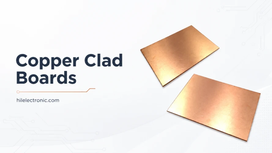
Copper Clad Boards (Copper-Clad Laminate): What They Are, Types, and How PCBs Are Made From Them
Figure 1. copper clad boards image for PCB manufacturing...
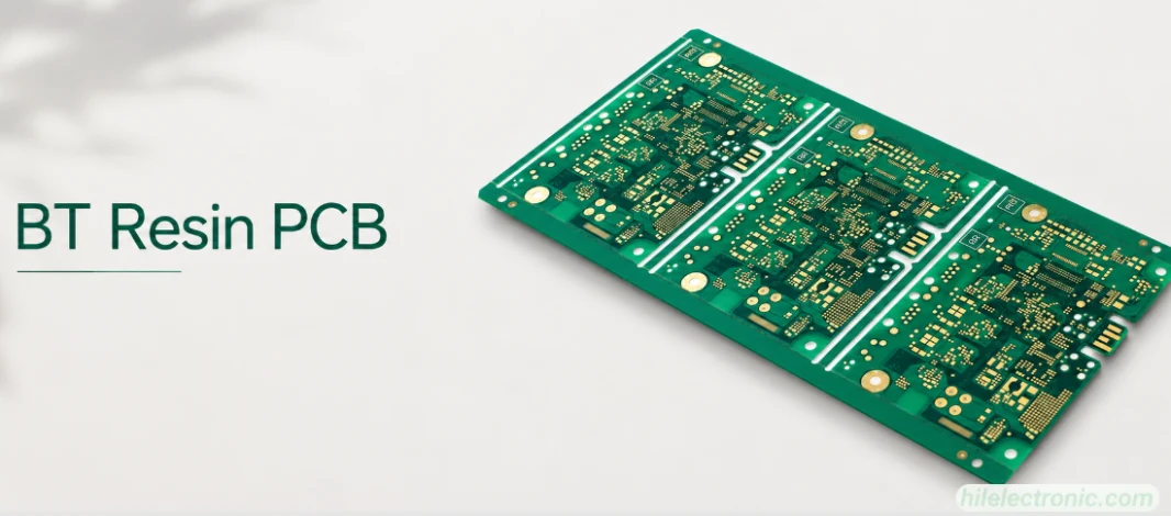
BT Resin PCB: Properties, Uses, and Fabrication Controls
Figure 1. BT resin PCB image for PCB manufacturing...
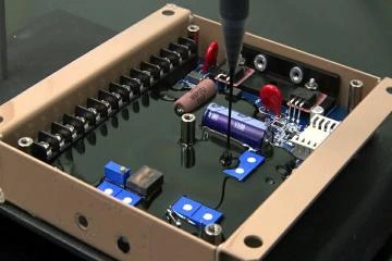
PCB Potting Services: Compounds, Process, and Design Rules
Figure 1. PCB potting services image for Highleap...
How to get a quote for PCBs
Let us run DFM/DFA analysis for you and get back to you with a report.
You can upload your files securely through our website.
We require the following information in order to give you a quote:
-
- Gerber, ODB++, or .pcb, spec.
- BOM list if you require assembly
- Quantity
- Turn time
In addition to PCB manufacturing, we offer a comprehensive range of electronic services, including PCB design, PCBA (Printed Circuit Board Assembly), and turnkey solutions. Whether you need help with prototyping, design verification, component sourcing, or mass production, we provide end-to-end support to ensure your project’s success. For PCBA services, please provide your BOM (Bill of Materials) and any specific assembly instructions. We also offer DFM/DFA analysis to optimize your designs for manufacturability and assembly, ensuring a smooth production process.