
Signal Integrity in Rigid-Flex PCB Design | Overcoming High-Speed Challenges

Signal integrity has become the defining challenge in modern rigid-flex PCB designs. As data rates climb into multi-gigabit ranges, even small discontinuities can cause reflections, jitter, and system instability.
Unlike conventional rigid boards, rigid-flex circuits must route high-speed signals across zones with different dielectric materials, stack-up geometries, and mechanical constraints—conditions that make maintaining electrical performance especially complex. This article explores the unique signal integrity issues in rigid-flex PCBs and the engineering strategies needed to overcome them.
Why Signal Integrity in Rigid-Flex PCB Design is Critical
In high-speed electronic systems, maintaining robust signal integrity is not optional—it is fundamental to ensuring reliable operation. Rigid-flex PCB designs present unique challenges compared with traditional rigid boards, as signals must navigate through zones with very different electrical and mechanical properties. Understanding why signal integrity matters is the first step toward designing boards that meet performance expectations without costly rework.
- High-Speed Sensitivity – At multi-gigabit data rates, even small discontinuities in a transmission line can trigger reflection, jitter, or timing errors.
- Rigid-to-Flex Transitions – Crossing between rigid and flexible zones introduces changes in dielectric constants and stack-up geometry, which heightens impedance mismatch risks.
- Electromagnetic Coupling – Limited shielding in flex regions and varying return paths increase vulnerability to EMI and crosstalk.
- Reliability Demands – In aerospace, medical, and automotive systems, even minor integrity issues can lead to critical system-level failures.
- Proactive Design Need – Signal integrity must be addressed early in the layout process with simulation, careful stack-up planning, and collaboration with manufacturing experts.
At Highleap Electronics, we specialize in advanced rigid-flex PCB manufacturing and assembly. By working closely with design engineers from the earliest stages, we help identify and mitigate potential signal integrity risks before they become production challenges. Our cross-industry experience shows that proactive planning is the key to ensuring successful high-speed rigid-flex implementations.
Core Challenges in High-Speed Rigid-Flex PCB Design
1. Maintaining Consistent Impedance Control
Impedance uniformity serves as the foundation of successful high-speed design. Any deviation from target impedance values causes signal reflections, degraded eye diagrams, and reduced noise margins. Rigid-flex circuits complicate this requirement because flexible dielectrics (typically polyimide-based) and rigid FR4 cores exhibit markedly different dielectric constants and loss tangencies.
Additionally, copper thickness variations between rigid and flex sections can disrupt controlled impedance lines, creating discontinuities that become increasingly problematic at higher frequencies.
2. Managing Rigid-to-Flex Transition Effects
The physical transition from rigid to flexible sections introduces unavoidable structural changes that impact electrical performance. Engineers often employ crosshatched or hatched ground planes in flexible zones to improve bendability and mechanical reliability.
However, these discontinuous planes interrupt current return paths and create localized impedance fluctuations. Transition regions must be meticulously engineered to minimize sudden electrical discontinuities while preserving the mechanical advantages of the flex design.
3. Electromagnetic Interference and Crosstalk Mitigation
High-speed signals in compact, multilayer rigid-flex layouts are especially vulnerable to EMI and crosstalk. Flexible zones provide limited ground reference area, which makes effective shielding more difficult.
In dense designs—such as medical implants, aerospace flight controls, or automotive sensor modules—maintaining adequate signal isolation is critical. As trace spacing shrinks to enable miniaturization, both near-end and far-end crosstalk can severely degrade signal quality.
4. Dielectric Thickness and Material Variability
Modern high-speed protocols—including PCIe Gen 4/5, USB 3.2/4.0, HDMI 2.1, and 10+ Gbps Ethernet—demand strict impedance control, typically targeting 50 Ω single-ended or 90–100 Ω differential impedance.
Achieving these precise values depends not only on trace geometry but also on tightly controlled dielectric thickness. Since rigid and flex regions utilize different substrate materials, adhesive systems, and coverlay constructions, maintaining thickness uniformity across the entire assembly presents a significant manufacturing challenge.

Signal Integrity
Design Strategies to Preserve Signal Integrity in Rigid-Flex PCBs
1. Advanced Impedance Control and Simulation
Utilize electromagnetic field solvers or specialized impedance calculators during the early design phase. Calculate and adjust trace width, spacing, and layer assignments across both rigid and flexible zones to compensate for material property differences. Perform sensitivity analysis to understand how manufacturing tolerances affect impedance variation.
Highleap Electronics provides impedance modeling support and manufacturing feedback to help designers optimize their stack-ups before committing to production.
2. Optimized Transition Design Techniques
Implement smooth tapering, gradual geometry changes, or staggered via patterns when routing high-speed signals between rigid and flexible sections. If crosshatched ground planes are necessary for flexibility requirements, utilize denser mesh patterns or employ alternative shielding methods to minimize return path disruption. Consider placing critical high-speed signals on layers that maintain more consistent reference planes across transitions.
3. Strategic Shielding and Reference Layer Planning
Incorporate dedicated shielding copper layers or specialized conductive films in high-speed signal zones. Conductive films offer lightweight EMI protection while preserving bend flexibility, whereas traditional copper shields deliver superior isolation performance at the cost of increased thickness and reduced flexibility. For differential pairs, ensure continuous, uninterrupted reference planes beneath signal traces throughout rigid-to-flex transitions.
4. Optimized Stack-Up and Material Selection
Select dielectric materials with predictable, stable dielectric constants (Dk) and low dissipation factors (Df) across the operating frequency range. Control adhesive layer thickness tightly, as adhesive variations significantly impact final impedance. Consider air-gap or adhesiveless constructions in flexible layers where appropriate—these approaches can help achieve more consistent impedance profiles while reducing overall stack-up stiffness and improving flexibility.
Practical Recommendations for Rigid-Flex PCB Design Success
1. Engage Manufacturing Partners Early
Collaborate with experienced PCB fabricators like Highleap Electronics during initial stack-up planning and impedance modeling phases. Early engagement helps identify potential manufacturing constraints and avoid costly redesigns late in the development cycle. Manufacturing Design for Excellence (DFX) reviews can catch issues before they reach production.
2. Prototype and Validate Rigorously
Build test coupons, impedance test structures, or limited production runs to empirically measure impedance accuracy, crosstalk levels, and EMI performance before committing to full-scale manufacturing. Time-domain reflectometry (TDR) and vector network analyzer (VNA) measurements provide invaluable validation data that simulation alone cannot capture.
3. Adhere to Industry Standards
Align your designs with established industry standards including IPC-6013 (qualification and performance specification for flexible/rigid-flex PCBs) and IPC-2141 (controlled impedance circuit boards and high-speed logic design). These standards codify best practices developed through decades of industry experience and help ensure both electrical performance and manufacturing reliability.
4. Embrace Iterative Refinement
Establish feedback loops combining electromagnetic simulation, prototype measurements, and manufacturing process data. Use these insights to continuously optimize both layout topology and material selection strategies. Document lessons learned and create design guidelines specific to your product family and performance requirements.
Conclusion
Rigid-flex PCBs unlock transformative form factor advantages and enhanced system reliability for today’s most demanding electronic applications. However, the signal integrity challenges inherent in high-speed rigid-flex design—ranging from impedance discontinuities to electromagnetic interference susceptibility—require significantly more sophisticated approaches than traditional rigid PCB design practices.
By combining precise electromagnetic modeling, disciplined transition region design, strategic material selection, and close collaboration with experienced manufacturing partners like Highleap Electronics, engineering teams can confidently deliver rigid-flex solutions that meet aggressive performance targets while maintaining excellent manufacturability and long-term reliability.
In all, effective rigid-flex PCB design requires both expertise and collaboration. Partner with Highleap Electronics for technical guidance, advanced manufacturing, and reliable delivery for even the most challenging projects.

Recommended Posts

NP-175F PCB Laminate for High-Reliability Multilayer Boards
NP-175F PCB laminate is a Nan Ya high-Tg, filled...

High CTI FR-4 PCB Manufacturing for Insulation-Critical Boards
High CTI FR-4 is used when a PCB design needs stronger...
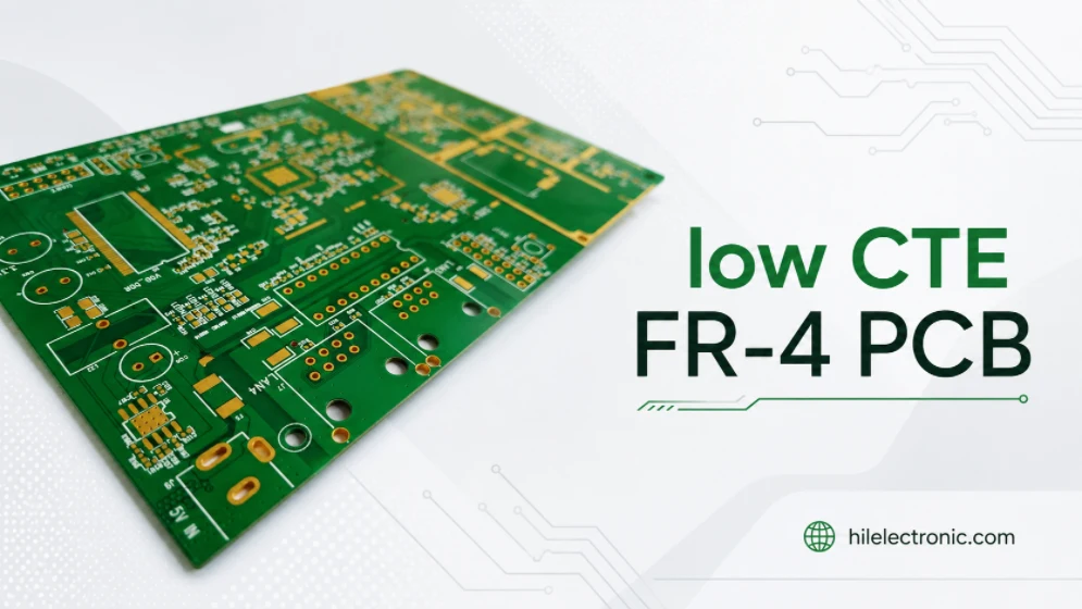
Low CTE FR-4 PCB Manufacturing for Through-Hole Reliability
Low CTE FR-4 PCB manufacturing is used when a circuit...
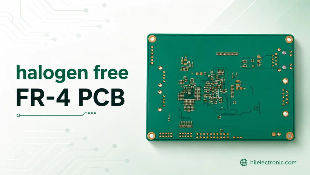
Halogen Free FR-4 PCB Manufacturing for Controlled Material Builds
Halogen free FR-4 PCB manufacturing is used when a product...
How to get a quote for PCBs
Let‘s run DFM/DFA analysis for you and get back to you with a report. You can upload your files securely through our website. We require the following information in order to give you a quote:
-
- Gerber, ODB++, or .pcb, spec.
- BOM list if you require assembly
- Quantity
- Turn time
In addition to PCB manufacturing, we offer a comprehensive range of electronic services, including PCB design, PCBA, and turnkey solutions. Whether you need help with prototyping, design verification, component sourcing, or mass production, we provide end-to-end support to ensure your project’s success.
For PCBA services, please provide your BOM (Bill of Materials) and any specific assembly instructions. We also offer DFM/DFA analysis to optimize your designs for manufacturability and assembly, ensuring a smooth production process.