
Advanced Rigid-Flex PCB Manufacturing Solutions

Rigid-Flex PCB manufacturing represents a sophisticated evolution in printed circuit board (PCB) technology, merging the strengths of both rigid and flexible substrates. This hybrid approach delivers unparalleled performance and versatility, making rigid-flex boards indispensable in a myriad of high-end electronic applications. Highleap Electronic provides cutting-edge rigid-flex PCB manufacturing and assembly for compact, reliable, and innovative electronic products.
Understanding Rigid-Flex PCB Manufacturing
Rigid-Flex PCBs are a revolutionary hybrid technology that merges the structural stability of rigid PCBs with the adaptability of flexible circuits. This combination enables the creation of advanced designs that take advantage of the strengths of both technologies.
Key Characteristics of Rigid-Flex PCBs
- Three-Dimensional Design Flexibility:
Unlike traditional rigid boards, Rigid-Flex PCBs can be bent, twisted, and folded during assembly and operation. This allows for the development of compact, space-efficient designs in confined or irregularly shaped enclosures. - Enhanced Reliability:
By eliminating the need for connectors and cables between rigid sections, Rigid-Flex PCBs reduce potential points of failure. This results in improved electrical performance and mechanical stability, even in high-stress or vibration-prone environments.
Rigid-Flex PCB manufacturing is a sophisticated process that combines the rigidity of traditional PCBs with the flexibility of flexible circuits. This unique blend enables the creation of compact, reliable, and durable electronic solutions that cater to complex, high-performance applications across various industries.
What Makes Rigid-Flex PCBs Unique?
Rigid-Flex PCBs consist of both rigid and flexible layers that are seamlessly integrated into a single structure. This integration allows for advanced designs with significant benefits:
- Space Optimization: The ability to design in 3D enables efficient use of space, making these PCBs suitable for compact and intricate devices.
- Enhanced Durability: The reduction of connectors and cables eliminates potential failure points, ensuring long-term reliability even in harsh conditions.
- Versatility: Rigid-Flex PCBs are ideal for dynamic applications requiring both structural stability and flexibility.
Overview of Rigid-Flex PCB Manufacturing
While rigid-flex PCB fabrication shares several similarities with traditional rigid PCB manufacturing, it introduces additional complexities due to the integration of flexible materials and multi-layered structures. The manufacturing process encompasses several critical stages, including material preparation, drilling, plating, etching, coverlay application, cutting, and lamination. Each step requires meticulous precision and control to ensure the final product meets stringent performance and reliability standards.
Key Steps in Rigid-Flex PCB Fabrication
1. Material Preparation and Layer Build-Up
The foundation of a rigid-flex PCB begins with the preparation of its flexible layers. Manufacturers start with either pre-laminated flexible substrates or bare polyimide (PI) films. The initial copper cladding is achieved by either laminating copper foil with a thin adhesive layer or chemically plating copper onto a seed layer using vapor deposition techniques, such as sputtering. This seed layer provides a base for subsequent copper plating, ensuring a strong and uniform foundation for circuit formation.
2. Adhesive/Seed Coating and Copper Foil Application
Adhesive lamination involves bonding copper foil to the flexible substrate using an epoxy or acrylic adhesive. For adhesiveless solutions, copper foil can be chemically plated directly onto the seed layer. Rolled annealed copper is often preferred for its flexibility and durability, enabling advanced fabrication processes that enhance overall product quality.
3. Drilling
Drilling is a critical step for creating vias, pads, and interconnects. Mechanical drilling is used for standard through-holes, while advanced laser drilling techniques, such as Excimer (ultraviolet) or YAG (infrared) lasers, are employed for creating microvias in high-density interconnect (HDI) designs. Larger cutouts are formed using hydraulic punching or blanking methods. Precise alignment during this step ensures seamless connectivity and structural integrity across both rigid and flexible sections.
4. Through-Hole Plating
The drilled vias are plated with copper to establish robust electrical connections and provide mechanical strength. The plating process, often referred to as “Cuposit,” ensures consistent copper thickness. Flexible areas typically require a plating thickness of at least 1 mil to enhance durability, compared to thinner plating in standard rigid PCBs.
5. Etch-Resist Application and Patterning
A photosensitive etch resist is coated onto the copper surfaces. A photomask is used to expose the desired circuit patterns onto the resist layer. The unprotected copper is chemically etched away, leaving the required circuitry intact. Finally, the etch resist is stripped, revealing the precise circuit layout.
6. Coverlay or Covercoat Application
To protect the exposed copper and enhance the mechanical stability of flexible sections, coverlay layers are applied. These layers are typically made from polyimide film with adhesive backing. In areas where soldering is required, the coverlay also serves as a solder mask to prevent solder bridging. Adhesiveless covercoats, such as photo-imageable solder masks, may also be used for finer designs, providing both protection and visual clarity.
7. Cutting and Shaping
Once the circuits are formed, the boards are cut and shaped according to the design specifications. For high-volume production, hydraulic punches and die sets are used for efficient blanking. Prototype or low-volume runs often employ blanking knives for greater precision and flexibility.
8. Lamination
Rigid and flexible layers are laminated together using heat, pressure, and additional adhesive layers. During this process, the flexible sections are framed within the rigid areas, ensuring they are securely bonded. For multi-layer designs, careful alignment is required to maintain electrical connectivity and prevent warping or delamination. The lamination process integrates all layers into a cohesive structure while preserving the flexibility of designated areas.
9. Electrical Testing and Final Inspection
Before shipment, the rigid-flex PCBs undergo rigorous testing to ensure functionality and reliability. Testing includes:
- Flying Probe Testing: Suitable for prototypes or low-volume production, verifying continuity and isolation.
- Automated Optical Inspection (AOI): Identifies surface-level defects such as misaligned components or broken traces.
- Electrical Testing: Ensures each connection meets the design specifications.
This stage is critical for ensuring that the boards meet the demanding requirements of their intended applications.
For production planning, it also helps to compare this topic with PCB solder mask requirements and Gerber and drill package before finalizing the fabrication or assembly package.
Advantages and Challenges of Rigid-Flex PCB Manufacturing
Advantages:
- Space and Weight Reduction: Combining rigid and flexible sections minimizes the overall size and weight of electronic assemblies, ideal for portable and compact devices.
- Enhanced Reliability: Reduced interconnections and robust construction lower the risk of circuit failures, especially in dynamic or harsh environments.
- Design Flexibility: Capable of accommodating complex geometries and high-density interconnects, rigid-flex boards enable innovative and space-efficient designs.
Challenges:
- Complex Manufacturing Process: The integration of multiple materials and layers requires advanced manufacturing techniques and stringent quality control.
- Higher Production Costs: Specialized equipment and materials, along with increased process steps, contribute to higher manufacturing expenses compared to traditional rigid PCBs.
- Lower Yield Rates: The intricate fabrication process may result in higher defect rates, necessitating thorough inspection and testing to ensure quality.
Conclusion
Rigid-Flex PCB manufacturing stands at the forefront of electronic innovation, offering a blend of rigidity and flexibility that meets the demanding requirements of modern technology. Despite the complexities and higher costs associated with their production, the benefits of reduced size, enhanced reliability, and design versatility make rigid-flex boards indispensable in numerous high-performance applications.
As electronic devices continue to evolve towards more compact and intricate designs, the role of rigid-flex PCB fabrication becomes increasingly critical. By leveraging advanced manufacturing techniques and collaborating with experienced rigid-flex PCB manufacturers, businesses can achieve superior product performance and maintain a competitive edge in the rapidly advancing electronics market.
For optimal results in rigid-flex PCB manufacturing, it is essential to partner with manufacturers who possess extensive expertise and state-of-the-art facilities. This collaboration ensures that each stage of the fabrication process—from design and material selection to assembly and quality assurance—is meticulously executed, resulting in high-quality rigid-flex boards that meet the exacting standards of today’s electronic applications.
FAQ: Rigid-Flex PCB Manufacturing
1. What factors influence the cost of Rigid-Flex PCB manufacturing?
The cost of Rigid-Flex PCB manufacturing is influenced by several factors, including the number of layers, material selection (such as adhesiveless vs. adhesive-based laminates), the complexity of the design, and the precision required for processes like drilling and plating. Additionally, customizations like special surface finishes or advanced testing protocols can add to the cost.
2. How does Rigid-Flex PCB manufacturing accommodate high-density designs?
Rigid-Flex PCBs are well-suited for high-density designs due to their ability to integrate multiple layers with complex interconnections in a compact space. The use of microvias, laser drilling, and precise lamination techniques allows for dense circuit layouts while maintaining electrical and mechanical reliability.
3. What industries benefit most from Rigid-Flex PCB manufacturing?
Industries that demand compact, reliable, and lightweight solutions benefit greatly from Rigid-Flex PCB manufacturing. These include aerospace, medical devices, automotive systems, military applications, and advanced consumer electronics. The boards’ flexibility and durability make them ideal for dynamic and harsh environments.
4. How does Rigid-Flex PCB manufacturing address reliability in harsh environments?
Rigid-Flex PCBs are designed to withstand harsh conditions by reducing the need for connectors and cables, which are prone to failure. The integrated design improves mechanical stability and electrical performance, and the use of durable materials like polyimide ensures resilience against thermal and mechanical stresses.
5. What is the role of testing in Rigid-Flex PCB manufacturing?
Testing is a critical step in ensuring the reliability and performance of Rigid-Flex PCBs. Advanced methods like flying probe testing, automated optical inspection (AOI), and electrical testing are employed to verify connectivity, continuity, and compliance with design specifications. These rigorous tests help minimize defects and ensure optimal functionality in end applications.
Get a Free PCB & PCBA Quote

Recommended Posts
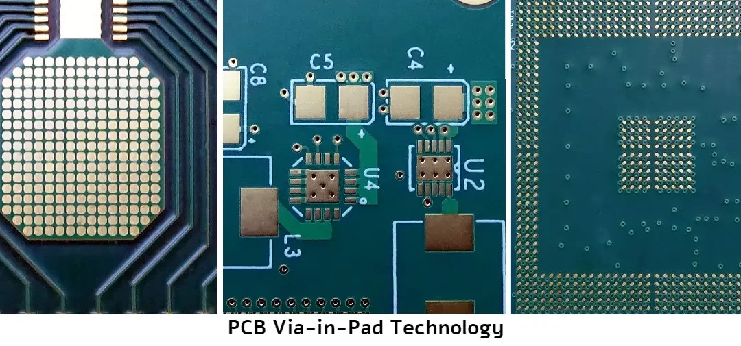
Comprehensive Analysis of PCB Via-in-Pad Technology
[pac_divi_table_of_contents...

PCB Hole Selection to Optimize PCB Performance and Cost
[pac_divi_table_of_contents...
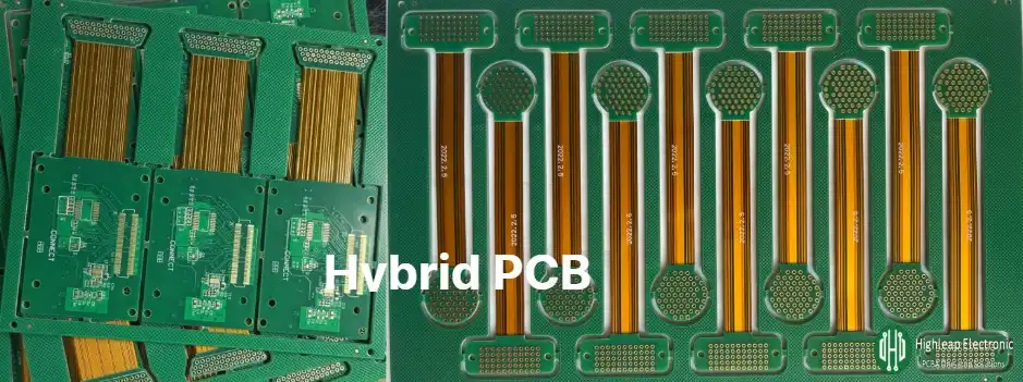
China High Quality Hybrid PCB Manufacturer
Hybrid PCB-Rigid flexible PCBIn the dynamic field of...

PCB Manufacturing Process Flow – Ultimate Guide Is Here
[pac_divi_table_of_contents...
How to get a quote for PCBs
Let us run DFM/DFA analysis for you and get back to you with a report.
You can upload your files securely through our website.
We require the following information in order to give you a quote:
-
- Gerber, ODB++, or .pcb, spec.
- BOM list if you require assembly
- Quantity
- Turn time
In addition to PCB manufacturing, we offer a comprehensive range of electronic services, including PCB design, PCBA (Printed Circuit Board Assembly), and turnkey solutions. Whether you need help with prototyping, design verification, component sourcing, or mass production, we provide end-to-end support to ensure your project’s success. For PCBA services, please provide your BOM (Bill of Materials) and any specific assembly instructions. We also offer DFM/DFA analysis to optimize your designs for manufacturability and assembly, ensuring a smooth production process.