
Rigid-Flex PCB Design Guidelines for Reliable Implementation

Understanding Rigid-Flex PCB Design and Layout Fundamentals
Effective Rigid-Flex PCB Design requires carefully dividing circuit functions between rigid and flexible sections based on component placement, electrical performance, and mechanical constraints. The transition zones between rigid and flexible areas are critical design boundaries where electrical continuity must be maintained despite differences in substrate flexibility and mechanical properties.
Component Placement Strategy
Components that need precise mechanical support—such as BGAs, QFNs, and high-pin-count connectors—should be placed in rigid sections, which provide dimensional stability, reliable solder joints, and better thermal management. Flexible sections handle routing and spatial requirements without the structural limits of rigid boards.
Transition Zone Management
The interface between rigid and flexible sections requires careful copper distribution and stress-relief features. Gradual copper tapering and teardrop-shaped pad-to-trace transitions help reduce mechanical stress and prevent copper cracking during repeated flexing, ensuring long-term reliability in Rigid-Flex PCB Design.
Advanced Routing Rules for Rigid-Flex PCBs
Rigid-flex PCB routing rules extend beyond conventional trace width and spacing requirements to encompass mechanical stress considerations and dynamic performance under flexion. Trace routing in flexible sections must account for both electrical performance and mechanical reliability across the expected operational flex cycles.
Directional Routing Requirements
Traces crossing bend areas should run perpendicular to the bend axis whenever possible, minimizing tensile and compressive stresses during flexion. Parallel routing to bend directions creates maximum stress concentration and should be avoided in critical signal paths. When parallel routing becomes unavoidable, trace spacing must be increased by 50-100% compared to rigid section requirements to accommodate material expansion and contraction.
Copper Distribution and Balancing
Maintaining uniform copper distribution across flexible sections prevents asymmetric stress development during bending operations. Unbalanced copper distribution can result in preferential bending directions and premature failure of traces on the tensile side of the flex. Design rules should specify maximum copper density variations of ±10% across the width of flexible sections.
Layer Transitions and Via Strategy
Via placement requires careful consideration of mechanical stress patterns, with strict avoidance of vias within bend radii. Transition vias connecting rigid and flexible sections should be positioned in rigid areas with adequate distance from bend initiation points, typically 0.5mm minimum from the rigid-flex boundary.

Rigid-Flex PCB
Bend Area Design and Mechanical Reliability
The mechanical design of bend areas is a critical aspect of Rigid-Flex PCB Design, affecting both electrical performance and long-term durability. Bend geometry must balance flexibility, electrical integrity, and manufacturability.
Critical Bend Radius and Standards
Rigid-flex PCB bend radius follows IPC-2223 guidelines, adjusted for material properties and application requirements. Single-layer flex sections typically require a minimum static bend radius of 6–10× thickness, while multilayer flex may need 12–20× thickness.
Dynamic vs. Static Bending
Repeated flexing demands larger bend radii. Dynamic applications generally require ≥20× thickness, with high-cycle uses exceeding 50×. Bend radius exponentially affects cycle life—doubling the radius can increase operational life by tenfold.
Material Considerations
Polyimide flex substrates (elastic modulus ~2.5 GPa) behave differently from FR-4 (~22 GPa). Designers must account for these differences in stress analysis and safety factors when calculating bend radii.
Stress Distribution and Optimization
Finite element analysis shows stress concentrates at neutral axis transitions and copper-substrate interfaces. Optimizing trace widths, via placement, and applying generous fillets reduces peak stress while maintaining connectivity.
Best Practices for Bend Area Design
- Use copper relief patterns or strain relief loops to reduce stress by up to 40% compared to straight traces.
- Ensure uniform coverlay adhesive thickness; adhesiveless polyimide can improve bend performance.
- Avoid sharp geometry transitions and apply gradual trace width changes in bend zones.
Impedance Control in Mixed-Substrate Rigid-Flex PCB Design
Effective Rigid-Flex PCB Design must address impedance challenges caused by differing dielectric properties of rigid and flexible substrates. Polyimide flex sections typically have dielectric constants of 3.2–3.5, while FR-4 rigid sections range from 4.0–4.5, creating potential impedance discontinuities at material transitions.
Dielectric Property Management
Adhesive layers in flexible sections add complexity, as their dielectric constants (≈2.9–3.2) differ from polyimide. Accurate impedance modeling requires precise stackup information, including adhesive thicknesses and material properties, which may vary by manufacturer and lot.
Differential Pair Routing
Maintaining consistent differential impedance across rigid-flex transitions requires trace geometry adjustments. Lower dielectric constants in flexible sections often necessitate 10–20% narrower trace widths or slightly increased spacing to achieve target impedance.
Transmission Line Continuity
Via transitions between rigid and flexible areas can cause impedance mismatches in high-speed circuits. Minimizing via stub lengths, using via-in-pad techniques where necessary, and ensuring continuous ground planes across transitions help maintain stable signal integrity.

HDI Rigid-Flex PCB
Via Design Strategies for Rigid-Flex PCB Design
Effective Rigid-Flex PCB Design requires specialized via strategies that balance electrical performance with mechanical reliability. Standard via rules must be adapted to accommodate the unique stress and manufacturing challenges of mixed-substrate constructions.
Mechanical Stress Considerations
Vias create stress concentration points in flexible areas, so placement is critical for long-term reliability. Circular vias disrupt the continuous substrate, forming potential failure points under bending. Guidelines recommend avoiding vias within bend radii and keeping a minimum distance of 0.254 mm from bend boundaries.
Manufacturing Process Adaptations
Via formation in rigid-flex boards requires modified drilling and plating processes to handle thermal expansion differences between rigid and flexible materials. Thermal mismatch between copper plating and polyimide can induce stress during thermal cycling, making specialized plating chemistry and process controls necessary.
HDI Integration Strategies
High-Density Interconnect (HDI) features, including microvias and blind vias, reduce board thickness and improve mechanical flexibility. Laser-drilled microvias in flex sections require precise process parameters to prevent substrate damage and ensure reliable plating adhesion.
Addressing Rigid-Flex PCB Design Challenges
Rigid-flex PCB design challenges encompass both technical and manufacturing considerations that require early collaboration between design and production teams. The complexity of these systems demands comprehensive Design for Manufacturing analysis to ensure both electrical performance and cost-effective production.
Thermal Management Integration
Thermal dissipation in rigid-flex assemblies requires careful consideration of heat conduction paths and thermal expansion mismatches. Copper pour strategies must balance electrical requirements with thermal performance while maintaining mechanical flexibility. Thermal vias in flexible sections present particular challenges due to the stress concentrations they create under thermal cycling conditions.
Testing and Validation Complexity
Electrical testing of rigid-flex assemblies requires specialized fixtures and procedures that can accommodate the three-dimensional nature of these boards. Traditional bed-of-nails testing approaches may not be feasible, necessitating alternative testing strategies such as boundary scan or embedded test points.
.jpg "Rigid Flex PCB printed circuit board(PCB)")
Rigid Flex PCB Printed Circuit Board (PCB)
Manufacturing Collaboration and DFM Optimization in Rigid-Flex PCB Design
Effective Rigid-Flex PCB Design relies on early collaboration between design teams and manufacturing partners to optimize performance, reliability, and producibility. The complexity of rigid-flex fabrication demands specialized capabilities that directly influence design feasibility and cost.
Material Selection and Availability
Material choices should be made with input from manufacturing partners to ensure compatibility and availability. Specialty materials may require longer lead times or minimum order quantities, affecting schedules and costs. Balancing material performance with manufacturing efficiency is key to reducing rigid-flex PCB costs.
Process Capability Verification
Manufacturing capabilities vary between suppliers, especially for complex rigid-flex designs. Early verification of bend radius limits, via aspect ratios, and impedance tolerances prevents costly design revisions. Clear specifications at the design stage ensure compatibility with production processes.
Stackup Optimization Strategies
Stackup design is a collaborative effort between electrical requirements and manufacturing constraints. Optimizing layer count, material selection, and thickness improves electrical performance and manufacturing yield. Partnering with experienced rigid-flex PCB manufacturing providers ensures the best balance between performance and cost.
Practical Implementation Guidelines for Rigid-Flex PCB Design
Successful Rigid-Flex PCB Design requires careful attention throughout the design process, from initial concept to final production validation. The following guidelines provide actionable steps to achieve reliable and manufacturable designs.
Establish Clear Design Rules
Define minimum bend radii, via placement restrictions, and trace width requirements early. Clear rules prevent downstream issues and ensure consistent implementation across design teams, aligning with manufacturing capabilities.
Stiffener Integration
PCB stiffeners provide mechanical support for component areas while maintaining assembly flexibility. Stiffener placement must coordinate with component layout and assembly processes. Material selection should consider thermal expansion and adhesive compatibility.
Test Point Accessibility
Flexible sections complicate traditional probe access for testing. Alternative approaches, such as edge connectors or embedded test features, ensure reliable test coverage without compromising the assembly.
Documentation and Communication
Comprehensive documentation communicates design intent to manufacturing partners. Assembly drawings should clearly indicate bend areas, stiffener locations, and handling requirements to prevent damage during production.
Quality Assurance and Validation Protocols
Rigid-flex PCB quality assurance extends beyond traditional PCB testing to include mechanical validation and long-term reliability assessment. These validation protocols ensure both immediate functionality and long-term operational reliability.
Mechanical Testing Requirements
Mechanical testing should validate both static bend performance and dynamic cycling capabilities where applicable. Bend testing protocols should match expected operational conditions while providing appropriate safety margins. Accelerated aging tests can predict long-term reliability under operational stress conditions.
Electrical Validation Procedures
Electrical testing must account for the three-dimensional nature of rigid-flex assemblies and potential variations in electrical characteristics under mechanical stress. Impedance measurements should be performed in both relaxed and stressed configurations to verify performance across operational conditions.
Conclusion
Rigid-Flex PCB design is a complex engineering discipline that integrates electrical and mechanical principles. Success requires early collaboration between design and manufacturing teams, careful attention to material properties and stress distribution, and systematic implementation of proven design practices, including layout, bend area, impedance, and via strategies.
Highleap Electronics offers comprehensive rigid-flex PCB design and manufacturing capabilities, including:
- Advanced stackup optimization and impedance control validation
- Mechanical reliability testing and bend area analysis
- Comprehensive DFM review to ensure manufacturability and yield
- Collaborative design support from concept through production validation
- Fast-turn rigid-flex PCB services for accelerated development cycles
- Process optimization for consistent electrical performance and mechanical reliability across production volumes
Our engineering team works closely with clients to transform complex design requirements into successful production outcomes, ensuring both immediate functionality and long-term reliability in demanding applications. Contact us today to start your Rigid-flex PCB project.

Recommended Posts
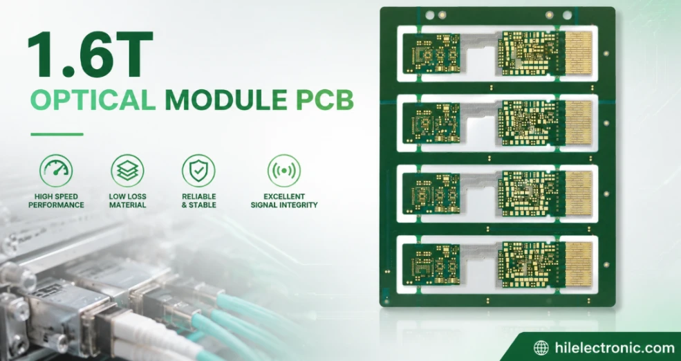
1.6T Optical Module PCB Manufacturing and Assembly Service
Table of contents1.6T Module Architectures and PCB...
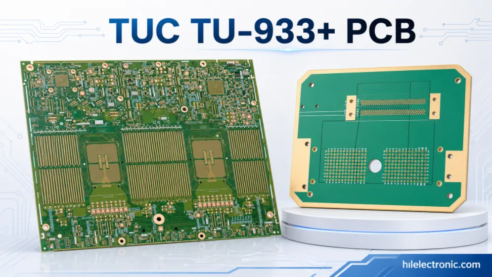
TUC TU-933+ PCB Manufacturing for Super-Low-Loss High-Speed Systems
Table of contentsWhat Is TU-933+ PCB Material?Why TU-933+...
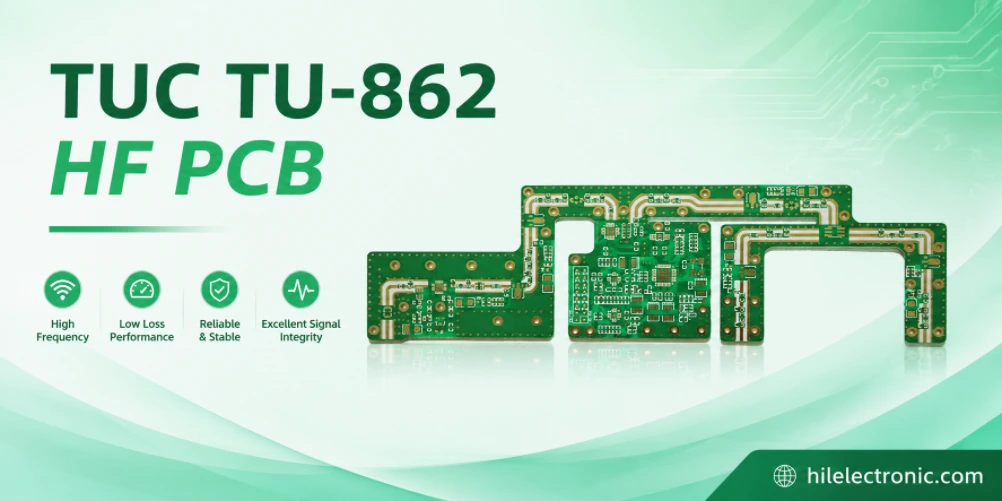
TUC TU-862 HF PCB Manufacturing and Assembly Service
Table of contentsWhat Is TU-862 HF?Why Choose TU-862 HF...
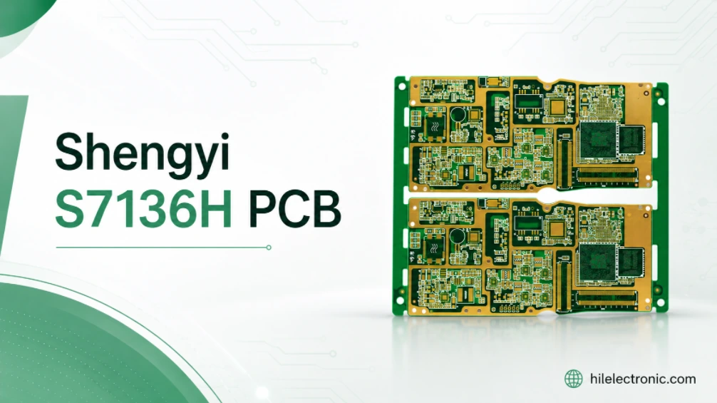
Shengyi S7136H PCB Manufacturing and Assembly Service
Table of contentsWhat Is a Shengyi S7136H PCB?Why...
How to get a quote for PCBs
Let‘s run DFM/DFA analysis for you and get back to you with a report. You can upload your files securely through our website. We require the following information in order to give you a quote:
-
- Gerber, ODB++, or .pcb, spec.
- BOM list if you require assembly
- Quantity
- Turn time
In addition to PCB manufacturing, we offer a comprehensive range of electronic services, including PCB design, PCBA, and turnkey solutions. Whether you need help with prototyping, design verification, component sourcing, or mass production, we provide end-to-end support to ensure your project’s success.
For PCBA services, please provide your BOM (Bill of Materials) and any specific assembly instructions. We also offer DFM/DFA analysis to optimize your designs for manufacturability and assembly, ensuring a smooth production process.