
Differential Pair Routing for High-Speed PCB Layout

Introduction
Differential pair routing represents a fundamental technique in high speed PCB layout design, utilizing two complementary signal traces to transmit data while maintaining superior noise immunity and signal integrity. In modern electronic systems, differential pairs are essential for high-speed interfaces including USB 3.x, PCIe, HDMI, Ethernet, DDR memory, and SerDes applications.
Proper differential pair routing directly impacts both signal integrity (SI) and electromagnetic interference (EMI) control, making it a critical consideration in high speed PCB design where data rates exceed 100 MHz and edge rates become increasingly aggressive.
Fundamentals of Differential Pair Routing
What Are Differential Pairs?
Differential pairs consist of two signal traces carrying complementary signals—one positive and one negative—that work together to transmit a single logical signal. The receiving circuit interprets the voltage difference between these two traces rather than the absolute voltage of either trace relative to ground.
This differential signaling approach provides inherent immunity to common-mode noise, power supply variations, and electromagnetic interference that would equally affect both traces.
Why Differential Pairs Are Critical in High Speed PCB Layout
In high speed circuit board applications, differential pairs offer several advantages over single-ended signaling. They provide enhanced noise immunity by rejecting common-mode interference, reduce electromagnetic emissions through balanced current flow, and enable higher data rates with improved signal integrity.
The differential nature allows for lower voltage swings while maintaining adequate noise margins, contributing to reduced power consumption and improved system reliability.
Key Design Considerations for Differential Pair Routing
Trace Spacing and Coupling
The spacing between differential pair traces determines the coupling strength and differential impedance characteristics. The widely accepted 3W rule suggests maintaining a minimum spacing of three times the trace width between differential pairs and adjacent signals to minimize crosstalk. However, within the differential pair itself, tight coupling is desirable to ensure balanced propagation and enhanced common-mode noise rejection.
This page is the routing guide for differential signals. For production release and fabrication notes, use high-speed PCB design for production; for impedance theory and practical matching, read impedance matching in high-speed PCB design; for a broader overview, start with high-speed PCB overview.
Intrapair spacing typically ranges from 0.1mm to 0.2mm, depending on the target differential impedance and stackup constraints. Closer spacing increases coupling but may present manufacturing challenges, while excessive spacing reduces coupling effectiveness and increases susceptibility to external interference.
Impedance Control
Differential impedance control requires precise management of trace geometry, stackup design, and high speed PCB materials selection. Target differential impedances commonly range from 85Ω to 100Ω, with 90Ω being standard for many high-speed interfaces. The differential impedance calculation involves trace width, spacing, dielectric thickness, and relative permittivity of the substrate material.
Modern impedance control in high speed PCBs requires careful stackup planning with controlled dielectric thicknesses and material selection. Low-loss dielectric materials with stable dielectric constants across frequency ranges are essential for maintaining consistent impedance characteristics throughout the signal bandwidth.
Length Matching
Length matching ensures temporal alignment of differential signal pairs, preventing skew-induced signal degradation. Acceptable length mismatch tolerances depend on signal rise times and system timing budgets, typically ranging from ±5 mil for aggressive high-speed designs to ±10 mil for more relaxed applications.
Precise length matching requires strategic routing techniques including serpentine tuning sections, preferably located away from sensitive analog circuits to minimize crosstalk. The tuning sections should maintain differential impedance characteristics while achieving the required length adjustments.
Via Usage in Differential Pairs
Vias introduce impedance discontinuities and parasitic effects that can degrade signal integrity in differential pair routing. Each via presents capacitive loading and inductive parasitic elements that affect signal propagation and impedance matching. Minimizing via count through strategic layer planning and utilizing blind or buried vias when necessary helps maintain signal integrity.
When vias are unavoidable, implementing via stitching techniques and maintaining symmetric via placement for both traces in the differential pair helps preserve signal balance and reduces mode conversion between differential and common modes.
Impact of Differential Pair Routing on SI and EMI
Improving Signal Integrity
Proper differential pair routing plays a key role in maintaining high signal quality. The balanced structure of differential signaling reduces common issues such as reflection, crosstalk, and timing skew, while also offering better noise immunity compared to single-ended signals.
- Noise immunity: Differential signals reject power supply noise and ground bounce.
- Controlled impedance: Tight coupling helps maintain consistent impedance and minimizes distortion.
- Lower skew: Equal-length routing reduces timing mismatches between signals.
- Resistance to SSN: Differential pairs perform well against simultaneous switching noise and system-level interference.
In summary, well-designed differential pairs ensure predictable, distortion-free transmission, which is essential for reliable high-speed systems.
Minimizing Electromagnetic Interference
Balanced differential pairs also help reduce EMI, as the equal and opposite currents in each trace naturally cancel out electromagnetic fields. This design approach is fundamental to achieving robust EMC compliance in high-speed PCBs.
- Field cancellation: Opposite current flows lower both radiated and conducted emissions.
- Ground plane design: Continuous ground beneath differential pairs provides a stable return path.
- Avoiding splits: Prevent routing across plane splits to reduce unexpected radiation sources.
- Predictable EMC behavior: Proper return path management minimizes unintended emissions.
In short, differential pair routing not only reduces electromagnetic emissions but also ensures compliance with EMC requirements for modern electronics.

Ensure differential pair routing is symmetrical with parallel signal paths
Best Practices for Differential Pair Routing
Implementing differential pair routing effectively requires following a structured set of principles:
1. Plan Early During Floorplanning
- Define routing corridors for differential pairs at the start of layout.
- Keep pairs away from high-noise sources such as clock lines or power switching regions.
2. Maintain Consistent Trace Geometry
- Use uniform trace width and spacing to control impedance.
- Ensure parallelism and tight coupling to maintain signal balance.
3. Use Gentle Routing Transitions
- Avoid sharp bends; apply smooth radius curves instead.
- If changes are necessary, apply symmetrical modifications to both traces to minimize mode conversion.
4.Preserve Return Path Continuity
- Keep differential pairs over a solid ground plane.
- Avoid crossing plane splits, which can disrupt impedance and increase EMI.
5. Optimize Layer and Via Usage
- Select layers with predictable impedance for differential pairs.
- Use vias sparingly and in symmetrical pairs to reduce parasitic effects.
By following a linear design process—plan, maintain geometry, route smoothly, preserve return paths, and optimize stackup—you ensure both signal integrity (SI) and electromagnetic compatibility (EMC) in high speed PCB layout.
Common Mistakes and How to Avoid Them
Even well-planned differential pair designs can fail if common pitfalls are overlooked. The following mistakes are the most critical to avoid in high speed PCB layout:
1. Length Mismatch
- Mistake: Differential pairs with length differences beyond system tolerance introduce timing skew and degrade signal quality.
- Solution: Apply precise length matching using serpentine traces or tuning structures to balance propagation delay.
2. Inconsistent Trace Geometry
- Mistake: Variations in spacing or width alter differential impedance and upset signal balance.
- Solution: Keep trace width and spacing uniform throughout the entire routing path to maintain consistent impedance.
3. Crossing Plane Splits
- Mistake: Routing across split reference planes interrupts return currents, creating impedance discontinuities and EMI risks.
- Solution: Plan the stackup carefully and ensure continuous reference planes under all differential traces.
4. Excessive Via Usage
- Mistake: Multiple vias add parasitic inductance and resistance, which degrade high-speed performance.
- Solution: Minimize via count by optimizing layer transitions and, where necessary, use symmetrical via pairs to preserve balance.
By recognizing and systematically avoiding these four mistakes—mismatched lengths, inconsistent geometry, plane splits, and excessive vias—designers can ensure differential pair routing delivers reliable signal integrity (SI) and robust electromagnetic compatibility (EMC).
Case Example: Differential Pair Design in USB 3.0 and PCIe
USB 3.0 SuperSpeed differential pairs require 90Ω ±10% differential impedance with length matching within ±5 mil. The high data rates (5 Gbps) demand careful attention to trace geometry, material selection, and via optimization. Strategic routing maintains signal integrity while accommodating the dense connector interfaces typical in USB implementations.
PCIe applications present even more stringent requirements with data rates reaching 32 Gbps in Gen5 implementations. Length matching tolerances tighten to ±2 mil or better, and via optimization becomes critical for maintaining signal integrity across multiple lanes. Advanced simulation and modeling techniques validate design performance before high speed PCB manufacturing to ensure specification compliance.
Conclusion
Differential pair routing in high speed PCB layout is more than just a design technique—it’s a discipline that determines how well a system maintains signal integrity and controls electromagnetic interference. Achieving success depends on precise attention to factors such as trace spacing, impedance consistency, length matching, and careful via usage.
When executed correctly, differential pair design delivers tangible benefits: stronger noise immunity, lower EMI emissions, and reliable signal performance in today’s high-speed, high-density applications.
Highleap Electronics provides comprehensive high speed PCB design and manufacturing capabilities including:
- Advanced impedance control and differential pair routing optimization
- Precise length matching and signal integrity analysis
- Low-loss material selection and stackup design
- Via optimization and advanced drilling technologies
- Comprehensive testing and quality assurance for high-speed applications
- EMI/EMC compliance validation and design support
Our experienced engineering team collaborates with customers to optimize differential pair routing strategies for specific application requirements while maintaining manufacturing efficiency and cost effectiveness. If you’re looking for reliable high speed PCB layout and manufacturing support, contact us today to discuss your project and see how we can help bring your design into production with confidence.
FAQ
1. What is the ideal impedance for differential pair routing?
The ideal differential impedance depends on the specific application and interface standard. Common targets include 90Ω for USB 3.x and many SerDes applications, 100Ω for Ethernet, and 85Ω for some DDR implementations. The key is maintaining consistency and meeting the target impedance within specified tolerances, typically ±10%.
2. How much length mismatch is acceptable in differential pairs?
Acceptable length mismatch varies with signal speed and system requirements. For moderate-speed applications (< 1 GHz), ±10 mil may be acceptable. High-speed designs often require ±5 mil or tighter, while extreme high-speed applications (> 10 Gbps) may demand ±2 mil or better matching to maintain timing integrity.
3. Can differential pairs cross split planes in PCB layout?
Differential pairs should avoid crossing split planes whenever possible, as this creates return path discontinuities and impedance variations. If unavoidable, stitching capacitors near the crossing point can help maintain return current continuity, though this approach requires careful analysis and adds component cost.
4. Which materials are best for differential pair routing in high speed PCB?
Low-loss dielectric materials with stable dielectric constants are preferred for high-speed differential pairs. Materials like Rogers RO4000 series, Isola I-Speed, or equivalent low-Dk/low-loss laminates provide excellent high-frequency performance. The specific material choice depends on frequency range, loss budget, and cost considerations for the particular application.

Recommended Posts
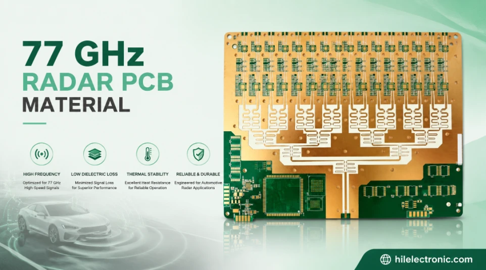
77 GHz Radar PCB Material Selection and Manufacturing Guide
Table of contentsWhat 77 GHz Changes in a PCBCommon 77 GHz...
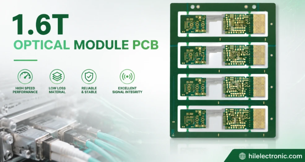
1.6T Optical Module PCB Manufacturing and Assembly Service
Table of contents1.6T Module Architectures and PCB...
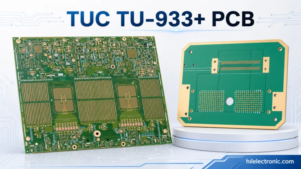
TUC TU-933+ PCB Manufacturing for Super-Low-Loss High-Speed Systems
Table of contentsWhat Is TU-933+ PCB Material?Why TU-933+...
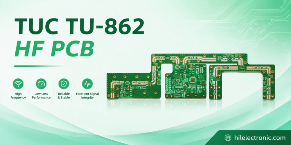
TUC TU-862 HF PCB Manufacturing and Assembly Service
Table of contentsWhat Is TU-862 HF?Why Choose TU-862 HF...
How to get a quote for PCBs
Let‘s run DFM/DFA analysis for you and get back to you with a report. You can upload your files securely through our website. We require the following information in order to give you a quote:
-
- Gerber, ODB++, or .pcb, spec.
- BOM list if you require assembly
- Quantity
- Turn time
In addition to PCB manufacturing, we offer a comprehensive range of electronic services, including PCB design, PCBA, and turnkey solutions. Whether you need help with prototyping, design verification, component sourcing, or mass production, we provide end-to-end support to ensure your project’s success.
For PCBA services, please provide your BOM (Bill of Materials) and any specific assembly instructions. We also offer DFM/DFA analysis to optimize your designs for manufacturability and assembly, ensuring a smooth production process.