
BGA and QFN Assembly With X-Ray Inspection for Hidden Solder Joints
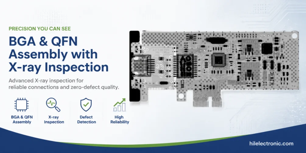
Table of contents
- Why Do BGA and QFN Assemblies Need Special Process Control?
- What PCB Design Details Are Reviewed for BGA and QFN?
- How Are Solder Paste and Stencil Apertures Selected?
- How Are BGA and QFN Components Stored and Reflowed?
- What Can X-Ray Inspection Detect?
- How Are BGA and QFN Assemblies Electrically Tested?
- What Are the Rework Limits for BGA and QFN?
- Request BGA and QFN Assembly Pricing
- BGA, QFN and X-Ray Inspection Questions
BGA and QFN assembly with X-ray inspection is required because critical solder joints are hidden beneath the component after reflow. Successful assembly depends on the relationship between the exact package, PCB land pattern, via structure, solder deposit, moisture condition, placement, board support, thermal profile and inspection plan.
Highleap Electronics reviews BGA, micro-BGA, QFN, LGA, CSP and similar bottom-terminated devices as part of the complete PCB assembly. Capability and inspection coverage are confirmed after reviewing the package and board. X-ray is used to answer defined questions; it is not a substitute for correct design, process control or electrical testing.
For quotation, send the PCB files, BOM and quantity. Highleap can identify the BGA and QFN parts from the BOM. Mention any required X-ray report, workmanship standard or reliability restriction if known; otherwise a practical inspection plan can be proposed during review.
1. Why Do BGA and QFN Assemblies Need Special Process Control?
BGA and QFN solder joints cannot be inspected with normal visual methods after assembly. Package warpage, via-in-pad construction, thermal-pad solder volume, moisture exposure and board copper distribution can create defects even when placement appears correct. Highleap reviews the complete joint system rather than qualifying a job from ball pitch alone.
| Package feature | Main manufacturing concern | Relevant control |
|---|---|---|
| BGA ball array | Hidden alignment, bridges, opens and warpage interaction. | Land/via review, placement, profile and X-ray. |
| Fine-pitch BGA/CSP | Small joints and reduced spacing. | Stencil/paste, board support and high-resolution inspection. |
| QFN/LGA perimeter joints | Hidden or partly visible joints with low stand-off. | Pad/mask review, paste balance and X-ray. |
| Large thermal pad | Excess solder, component float and void pattern. | Segmented aperture, profile and acceptance criteria. |
| Thin board or large package | Package and PCB warpage during reflow. | Panel support, copper balance and thermal route. |
Customers can review BGA package and assembly considerations and BGA versus QFN differences, but Highleap’s manufacturing decision is based on the exact manufacturer part number and PCB data.
2. What PCB Design Details Are Reviewed for BGA and QFN?
Land dimensions, solder-mask definition, fanout, via-in-pad, copper balance, surface finish, board thickness and local support affect solder formation. Highleap checks whether the PCB data and package drawing are compatible and whether the panel can be printed, placed, reflowed and X-rayed effectively.
- Confirm pad size, pitch and solder-mask relationship.
- Review dog-bone or via-in-pad fanout and whether vias are filled/capped as required.
- Check QFN thermal-pad aperture and via pattern.
- Review local copper concentration and expected thermal mass.
- Confirm fiducials, board support and panel flatness around the device.
- Identify shielding, connectors or nearby components that may obstruct X-ray views.
A focused PCB DFM review for hidden-joint packages should identify the exact design risk and possible action. Highleap does not require the buyer to submit a separate technical package beyond the normal board files and BOM unless a special reliability or acceptance condition applies.
3. How Are Solder Paste and Stencil Apertures Selected?
The solder deposit must support both the bottom-terminated package and surrounding components. For QFN thermal pads, a single large opening may deposit too much paste and increase float or voiding. For fine-pitch BGA or CSP, deposit consistency and board support become critical.
| Application | Stencil consideration | Objective |
|---|---|---|
| BGA with standard balls | Stable paste transfer and alignment support. | Consistent joint formation without bridges or insufficient solder. |
| Fine-pitch BGA/CSP | Area ratio, aperture release and print stability. | Reduce deposit variation at small features. |
| QFN thermal pad | Segmented/window-pane aperture. | Control total volume and provide outgassing paths. |
| Mixed package board | Localized aperture modification or step stencil. | Balance small and large solder-volume requirements. |
| Via-in-pad | Via treatment and aperture strategy. | Prevent solder loss and joint inconsistency. |
Highleap can use SMT stencil aperture planning and paste-volume inspection for BGA and QFN deposits where the package risk and volume justify measurement. These controls should be matched to the board rather than offered as marketing terms.

4. How Are BGA and QFN Components Stored and Reflowed?
Moisture-sensitive packages can be damaged by uncontrolled storage or repeated thermal exposure. Highleap reviews packaging condition, moisture sensitivity, floor-life status and any need for controlled baking. Customer-supplied parts should arrive in identifiable, machine-compatible packaging with enough overage for setup.
Reflow must support the paste alloy, component limits, board thermal mass and warpage behavior. A controlled reflow soldering profile considers ramp, soak, time above liquidus, peak and cooling rather than relying only on one temperature number.
- Verify exact package and moisture condition before setup.
- Store and handle the parts under the agreed controls.
- Print and inspect the solder deposit as required.
- Place using verified package data and board alignment.
- Reflow with a representative profile and stable panel support.
- Inspect the first representative units before releasing the full quantity.
Where a package or board combination has unusual risk, Highleap may recommend a first-lot trial, added inspection or a customer-approved limitation before committing repeat-production pricing.
5. What Can X-Ray Inspection Detect?
X-ray inspected PCB assembly can reveal hidden solder features that are not visible from the component edge. Depending on equipment and package geometry, X-ray may show alignment, solder bridges, missing or abnormal joints, gross opens, void distribution and solder-ball consistency. It cannot by itself prove electrical continuity, metallurgical strength or long-term reliability.
| X-ray question | Possible observation | Additional evidence that may be needed |
|---|---|---|
| Is the package aligned? | Ball/pad pattern and package position indicators. | First-article placement records. |
| Are there hidden bridges? | Connected solder areas between adjacent joints. | Electrical short testing and process review. |
| Are joints missing or abnormal? | Low-density, irregular or absent solder features. | Electrical test, cross-section or failure analysis if required. |
| Is QFN voiding controlled? | Void location and approximate distribution. | Customer-defined acceptance method and thermal/reliability context. |
| Is every joint reliable? | X-ray cannot directly answer this. | Process validation, test and reliability evidence. |
Highleap can provide PCB X-ray inspection services with the coverage defined in the quote. The customer should specify any formal acceptance requirement; otherwise Highleap can recommend first-article, sampling or broader inspection based on package risk.
6. How Are BGA and QFN Assemblies Electrically Tested?
Because X-ray has limitations, hidden-joint inspection should be combined with electrical or functional evidence. Flying probe or ICT may detect opens and shorts when test access exists. Functional testing confirms that the board operates through the relevant circuits and firmware.
SPI, placement verification, profile and X-ray.
Continuity, isolation, flying probe or ICT within available coverage.
Power, communication and application-specific operation.
Link the unit or lot to materials, process and test results when required.
Highleap can combine PCB functional testing and PCB electrical testing methods with BGA/QFN assembly. The test level should reflect product risk and volume; not every project requires a dedicated fixture on the first prototype lot.
The electrical test should be selected according to available access and product risk. Highleap can begin with a basic continuity or functional check for an early lot and introduce dedicated ICT or fixture-based coverage when the design and production quantity justify it.
7. What Are the Rework Limits for BGA and QFN?
BGA and QFN rework introduces another thermal cycle and local heating to the component and PCB. Before production, the customer and Highleap should agree whether rework is permitted, how many attempts are allowed, what inspection follows and when a board must be rejected.
| Rework decision | Factors to consider | Required follow-up |
|---|---|---|
| Local lead/QFN edge touch-up | Joint accessibility and workmanship acceptance. | Visual or X-ray review and electrical retest. |
| QFN replacement | Pad condition, thermal-pad cleaning and board sensitivity. | Controlled profile, X-ray and full functional retest. |
| BGA replacement | Package condition, pad integrity, warpage and prior thermal history. | Professional rework process, X-ray and electrical/functional retest. |
| Repeated failure | Risk of pad damage or unresolved design/process cause. | Stop rework and perform engineering disposition. |
Highleap can review BGA rework and replacement and BGA solder-joint risks. Rework should be visible in the production record when the customer requires unit-level history.
8. Request BGA and QFN Assembly Pricing
Send the PCB files, BOM and quantity. Highleap can identify bottom-terminated packages and return any package-specific questions. Add your X-ray, test or rework restrictions when they exist; otherwise the quotation can propose a practical default scope.
The response should define sourcing, stencil assumptions, moisture handling, first-article controls, reflow, X-ray coverage, test and rework boundaries. Capability remains conditional on the exact package and board construction.
Use the BGA and QFN PCB assembly quote form to begin. Highleap can quote prototypes, NPI, pilot and repeat production with the same package-specific manufacturing plan.
Highleap can also specify whether X-ray images, summary results or exception reports are included. This prevents the customer from assuming that a general X-ray process automatically includes a formal report for every device.
9. BGA, QFN and X-Ray Inspection Questions
Does X-ray guarantee every BGA joint is good?
No. X-ray provides valuable hidden-joint evidence but cannot directly prove electrical continuity, metallurgy or long-term reliability. It should be combined with controlled assembly and appropriate electrical or functional testing.
Is 100% X-ray required for every BGA and QFN order?
Not always. Coverage may be first-article, sampling or full-lot depending on package, design, product risk and customer requirement. Highleap states the proposed coverage in the quote.
Can QFN voids be completely eliminated?
Usually not. The objective is to control void location and extent relative to thermal, electrical and customer acceptance requirements. Stencil pattern, via design, paste and reflow all influence the result.
Can customer-supplied BGA components be assembled?
Yes, subject to package identity, moisture condition, quantity, packaging and rework history. Highleap will review receiving and handling requirements before confirming the build.
What does a BGA PCB assembly X-ray inspection plan include?
A BGA PCB assembly X-ray inspection plan defines which packages and units are inspected, the defects or measurements being reviewed, acceptance criteria, result records and escalation when an abnormal pattern is found.
Can one QFN PCB assembly service also provide BGA QFN soldering services?
Yes. A QFN PCB assembly service can be integrated with BGA QFN soldering services on the same SMT route. Package-specific stencil, via, moisture, profile and X-ray controls are still required.
What should a BGA assembly manufacturer confirm before quotation?
A BGA assembly manufacturer should confirm the exact package, board land/via construction, panel, component condition, inspection coverage, test and rework restrictions before committing capability and schedule.
What is bottom terminated component assembly?
Bottom terminated component assembly covers packages whose primary joints are under the body, including BGA, QFN, LGA and many CSP devices. Process and inspection must account for limited visual access.

Recommended Posts

TMM4 Filter PCB Manufacturing
TMM4 filter PCB manufacturing is controlled by the...

TMM3 PCB Manufacturing for RF Modules
TMM3 PCB manufacturing is most useful where the RF module...

TMM6 PCB Fabrication
TMM6 fabrication is the process-control page for a mid-Dk...

TMM10 PCB Manufacturing for Compact RF Designs
Table of contentsHow TMM10 Shrinks RF StructuresTMM10 vs...
How to get a quote for PCBs
Let’s run DFM/DFA analysis for you and get back to you with a report. You can upload your files securely through our website. We require the following information in order to give you a quote:
-
- Gerber, ODB++, or .pcb, spec.
- BOM list if you require assembly
- Quantity
- Turn time
For PCBA services, please provide your BOM (Bill of Materials) and any specific assembly instructions. We also offer DFM/DFA analysis to optimize your designs for manufacturability and assembly, ensuring a smooth production process.