
Stencil Aperture Design Guideline for Cost Efficient PCBA

Table of Contents
- Stencil aperture design fundamentals
- Area ratio and aspect ratio rules
- Aperture optimization for components and thermal pads
- Stencil cost factors and what to send your assembler
At Highleap Electronics, we manufacture PCBs and run SMT assembly builds every day. Stencil design is not only a quality topic, it is also a cost topic. The right aperture strategy prevents rework and line delays, while the right stencil specification avoids paying for options you do not need. This guide explains practical stencil aperture rules and the real cost drivers that buyers care about.
Stencil aperture design fundamentals
A solder paste stencil transfers paste onto PCB pads during printing. The stencil aperture is the opening that defines where paste is deposited and how much paste is released. Even when your PCB layout is correct, a poor aperture strategy can cause insufficient paste, excessive paste, bridging, solder balling, or component float during reflow.
How paste transfer works
- Squeegee rolls solder paste across the stencil surface
- Paste fills each aperture opening
- Stencil separates from the PCB
- Paste releases from aperture walls and deposits on pads
Key variables that drive print results
- Aperture size opening dimensions may be reduced or modified compared to pad size
- Stencil thickness directly drives volume commonly 0.10mm to 0.15mm depending on pitch and part mix
- Aperture shape rectangle rounded corners home plate window patterns
- Wall quality smoother walls improve release and reduce cleaning frequency
Paste volume calculation
Paste Volume = Aperture Area × Stencil Thickness
Example: 0.5mm × 1.0mm aperture, 0.12mm stencil
Volume = 0.5 × 1.0 × 0.12 = 0.06mm³ = 60 nanoliters
If you are preparing a complete handoff package for PCB assembly, stencil decisions should align with your full manufacturing dataset. This checklist helps avoid missing or mismatched files:
Assembly file requirements.
Area ratio and aspect ratio rules
Two ratios predict whether paste will release cleanly from the aperture. When ratios are too low, paste sticks to aperture walls and deposits become inconsistent. That is when buyers pay twice, first for a stencil that prints poorly, and then for rework, cleaning time, and production delays.
Area ratio
Area Ratio = Aperture Area / Wall Area
For rectangular aperture
Area Ratio = (L × W) / [2 × T × (L + W)]
L = length W = width T = stencil thickness
| Area ratio | Paste release expectation | Production meaning |
|---|---|---|
| >0.66 | Strong margin | Standard stencil and stable printing |
| 0.50 to 0.66 | Workable with tuning | May need thinner stencil or shape optimization |
| <0.50 | High risk | Often needs step stencil or process upgrade |
Aspect ratio
- >1.5 excellent release margin
- 1.0 to 1.5 workable with good stencil quality and process control
- <1.0 often unstable release consider thinner stencil or step down
Aperture optimization for components and thermal pads
In PCB assembly, using a 1 to 1 aperture to pad rule everywhere is rarely optimal. The goal is to put the right paste volume on the right pads while minimizing bridging, voiding, and component float.
Aperture reduction
- Thermal pads reduce total coverage to prevent floating and help outgassing
- Via in pad reduce opening to limit paste wicking into vias
- Tombstone control balance deposits between chip pads when one side is more thermally dominant
Aperture enlargement
- Gull wing and J lead may need controlled increase for fillet formation
- Large connector leads may need more volume depending on lead mass
- Pin in paste through hole reflow requires engineered paste in holes
Aperture shape optimization
- Rounded corners improves release for small apertures and reduces paste sticking
- Home plate often used on fine pitch leads to reduce bridging risk
Thermal pad windowing strategy
- Total coverage typically 50 to 80 percent of pad area
- Pattern multiple small windows instead of one solid opening
- Window gaps provide outgassing paths and reduce voiding risk
- Edge clearance keep paste back from pad edge to reduce squeeze out
Stencil cost factors and what to send your assembler
Many buyers ask a simple question, how much does a solder paste stencil cost. The real answer depends on your PCB and the stencil specification. In PCB assembly, the lowest stencil price is not always the lowest total cost if it causes unstable printing, extra cleaning, or rework. Below are the cost drivers that matter most in real production.
Main stencil price drivers
- Stencil type framed stencils cost more than frameless stencils but are faster on production lines
- Stencil thickness unusual thickness can increase cost and lead time especially when the supplier does not stock it
- Step stencil step down or step up regions increase price because of extra machining and tighter process control
- Fine pitch capability very small apertures may require higher quality cutting finishing or specialty stencil processes
- Nano coating adds cost but can reduce paste sticking and cleaning time on small apertures
- Order volume prototype one off stencils cost more per piece than repeated builds
How to reduce stencil cost without increasing assembly risk
- Use a standard thickness when your smallest pitch allows it instead of forcing a step stencil
- Reserve step stencils for true mixed pitch boards where fine pitch and large power parts coexist
- Use aperture shape optimization before paying for specialty stencil options
- Share your component pitch and smallest pad sizes with the assembler so they choose the most cost effective thickness
Information to send for accurate stencil pricing and review
- Gerber paste layers top and bottom
- Board outline and panelization information if applicable
- Key component list focusing on minimum pitch QFN QFP BGA and miniature passives
- Any known issues such as tombstoning or bridging from past builds
Stencil and print risk should be reviewed as part of a manufacturability process. Our engineers include stencil related checks in the overall build readiness review:
free DFM review.
Stencil choices also depend on PCB assembly rules such as fiducials keep outs and panel strategy. For a practical assembly focused checklist see:
PCB assembly design rules.
Contact Highleap Electronics for stencil aperture optimization and a cost focused recommendation. Sharing your paste layer Gerbers plus the minimum pitch on your PCB helps us propose a stencil thickness and aperture strategy that balances price and yield.
Helen supports international engineering teams with end-to-end PCB fabrication and assembly solutions, helping projects move from quick-turn prototypes to stable mass production. Her experience spans high-frequency and RF boards, complex multilayer stackups, rigid-flex, and flex PCB technologies across multiple industries. By translating technical requirements into practical manufacturing plans, she helps customers improve manufacturability, reduce risk, and optimize cost and lead time—while maintaining consistent quality at scale.
at Highleap Electronics

Recommended Posts

Wireless Mechanical Keyboard PCB Manufacturing
Table of contentsWireless Keyboard PCB Procurement...

Split Keyboard PCB Manufacturing & Assembly
Table of contentsSplit Keyboard PCBA Procurement...
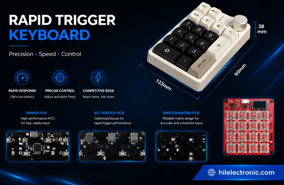
Rapid Trigger Keyboard PCB Manufacturing & PCBA
Table of contentsRapid Trigger PCBA Buying and Performance...
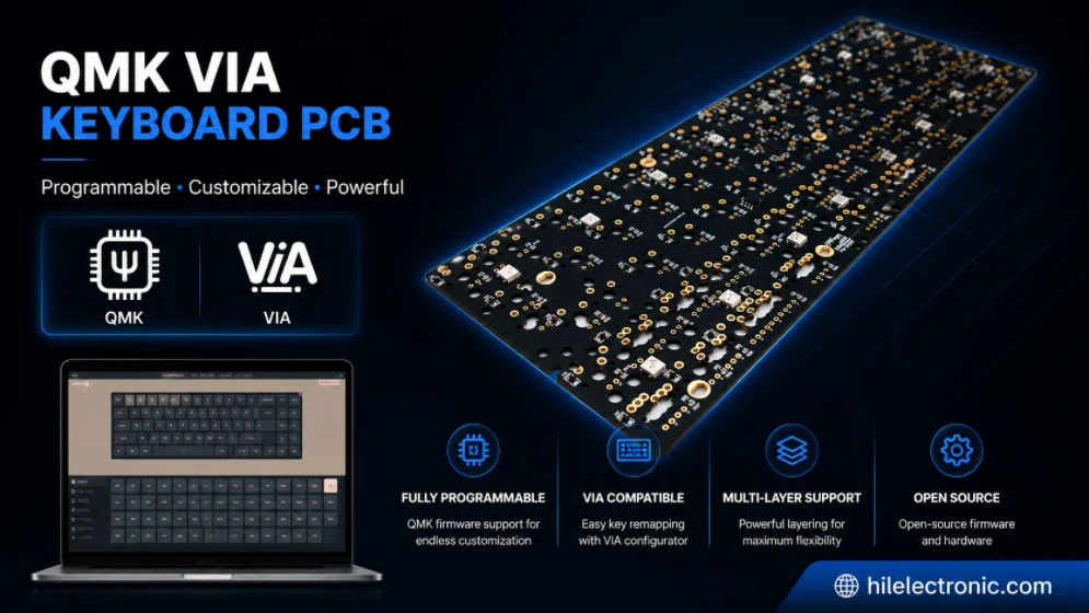
QMK/VIA Keyboard PCB Manufacturing & Assembly
Table of contentsQMK/VIA Keyboard PCB Buying...
How to get a quote for PCBs
Let us run DFM/DFA analysis for you and get back to you with a report.
You can upload your files securely through our website.
We require the following information in order to give you a quote:
-
- Gerber, ODB++, or .pcb, spec.
- BOM list if you require assembly
- Quantity
- Turn time
In addition to PCB manufacturing, we offer a comprehensive range of electronic services, including PCB design, PCBA (Printed Circuit Board Assembly), and turnkey solutions. Whether you need help with prototyping, design verification, component sourcing, or mass production, we provide end-to-end support to ensure your project’s success. For PCBA services, please provide your BOM (Bill of Materials) and any specific assembly instructions. We also offer DFM/DFA analysis to optimize your designs for manufacturability and assembly, ensuring a smooth production process.