
What Is High-Speed PCB? Design and Manufacturing Guide

Modern electronic systems require sophisticated high speed PCB solutions that integrate precise impedance control, advanced material science, and specialized manufacturing processes. This comprehensive guide examines the complete engineering lifecycle of high speed PCBs, from initial design considerations through final production validation, providing insights essential for engineers developing cutting-edge electronic systems.
What Defines High Speed PCB Technology?
High speed PCB technology comes into play when signal behavior is governed more by electromagnetic propagation than by simple electrical connectivity. This typically occurs once signal rise times are shorter than twice the electrical delay of the transmission path—often at frequencies above 1 GHz or edge rates faster than 1 nanosecond.
Fundamental Characteristics
High speed PCBs differ from conventional boards through several key features. Controlled impedance is essential for maintaining signal integrity, requiring precise trace dimensions and stable dielectric properties. Layout rules focus on reducing reflections, crosstalk, and electromagnetic interference to ensure reliable high speed designs.
Power integrity is equally critical. Fast switching currents can destabilize supply voltages, so the power distribution network must maintain low impedance across wide frequency ranges with effective local decoupling near active components.
Performance Requirements
Modern high speed circuit board applications demand strict performance standards. Impedance control is typically held within ±5% to ±10%. Insertion loss must stay within defined limits across the working frequency range. Timing skew also requires careful management, with differential pair and bus routing often length-matched within 0.1 mm for high-speed memory and data interfaces.
High Speed PCB Design Fundamentals
Effective high speed PCB design requires analyzing signal propagation and optimizing key electrical parameters. Design strategies must address transmission line effects, electromagnetic compatibility, and manufacturing limits from the start of development.
Signal Modeling and Simulation
Successful high speed PCB design relies on accurate signal integrity analysis. Time-domain models predict reflections and impedance discontinuities, while frequency-domain simulations assess insertion loss and crosstalk. Power integrity analysis defines target impedance and guides decoupling placement, ensuring stable voltage under fast switching conditions.
Stackup Architecture and Layer Planning
Stackup planning is central to high speed PCB performance. Signal layers should be paired with reference planes to maintain controlled impedance. Mixed-signal boards often use isolated ground planes with selective bridging to reduce noise. HDI structures improve routing density while minimizing stub effects and via-induced distortion.
Material Selection and Properties
High speed PCB materials directly influence signal quality. Stable dielectric constants support consistent impedance, while low dissipation factors reduce insertion loss. FR4 works up to about 5 GHz with careful design, but advanced laminates like Rogers RO4000, Megtron, or Isola I-Speed are preferred for higher-frequency applications. For designs above 10 GHz, low-loss materials become essential to preserve timing and amplitude margins.
Advanced Routing Techniques
High speed signal routing requires strict control. Differential pair routing improves noise immunity for PCIe, USB, and other serial standards. Length matching ensures timing accuracy, typically within 0.05 mm for clocks and 0.25 mm for data lines. Serpentine routing adjusts trace lengths while limiting crosstalk. Via optimization and back-drilling reduce stubs and maintain signal integrity in demanding high speed designs.

IT-988G High-Speed PCB
High Speed PCB Manufacturing Excellence
High speed PCB manufacturing combines advanced materials, precision fabrication, and strict quality control. Manufacturing capability ultimately decides whether design intent delivers reliable electrical performance in volume production.
Use this page for the high-speed PCB overview. When the design moves from concept to layout, check differential pair routing and impedance matching in high-speed PCB design; for release-to-fabrication decisions, the high-speed PCB design for production page covers production review in more detail.
Advanced Fabrication Processes
Modern high speed PCB manufacturing relies on processes that ensure dimensional accuracy and signal integrity. Laser drilling enables microvias down to 0.075 mm with excellent plating reliability. Sequential build-up supports HDI constructions with stacked or staggered vias, while semi-additive processing achieves fine-line capabilities below 25 μm. Controlled lamination cycles with vacuum assist secure uniform dielectric thickness and eliminate voids for stable performance.
Material Processing and Control
High speed PCB manufacturing requires careful handling of low-loss laminates, which may be less thermally stable than standard FR4. Prepreg flow must be controlled for consistent dielectric thickness and adhesion. Certified material lots ensure dielectric constant variation within ±0.05. Copper surface treatments balance adhesion strength with low conductor roughness to minimize insertion loss.
Precision Measurement and Verification
Quality assurance focuses on verifying signal integrity. Impedance control in high-speed PCBs is validated using time-domain reflectometry with ±1 ohm accuracy. AOI systems inspect fine-line geometries, while X-ray imaging detects voids and registration errors. Statistical process control tracks impedance, via registration, and surface finish, enabling predictive quality management and stable yields.
Environmental and Reliability Considerations
High speed PCB reliability depends on managing environmental stress. Low-loss laminates require dry storage to prevent moisture-driven delamination. Thermal cycling must withstand lead-free soldering without warpage, supported by materials with matched CTE values. Copper grain refinement and controlled annealing reduce resistance variation, improve current capacity, and enhance long-term durability.
High Speed PCB Assembly Considerations
High speed PCB assembly requires specialized techniques to preserve signal integrity and ensure reliable connections. Key factors include precise component placement, controlled soldering, and effective thermal management.
Component Placement and Orientation
High speed component placement accuracy is critical for processors, memory, and transceivers. BGA devices demand precision within ±25μm to secure stable solder joints and maintain impedance control. Proper component orientation shortens trace lengths, improves EMI performance, and ensures thermal balance. Decoupling capacitors should be placed close to IC power pins with optimized vias to reduce inductance and enhance power delivery.
Advanced Assembly Processes
High speed PCB soldering processes, especially reflow, must balance heat profiles for mixed components. Optimized stencils and nitrogen reflow help reduce solder voids and improve joint reliability. For mixed-technology boards, selective soldering provides controlled heat transfer, avoiding thermal stress on sensitive areas.
Thermal Management Integration
High speed PCB thermal management addresses rising power densities and switching speeds. Thermal interface materials and heat spreaders enhance conductivity while maintaining electrical isolation. Placement strategies and airflow design minimize hotspots, supported by simulation to validate performance under peak loads.

High Speed PCB
Verification and Testing Methodologies
High speed PCB testing and verification ensure performance consistency and compliance with design standards. Methods cover electrical validation, process verification, and reliability testing under environmental stress.
Electrical Performance Validation
Signal integrity testing with time domain reflectometry (TDR) detects impedance discontinuities and profiles transmission lines. Network analyzer measurements confirm insertion loss, return loss, and crosstalk, while S-parameter analysis validates simulation accuracy. High-speed digital tests, including bit error rate and eye diagram analysis, assess data quality under real conditions.
Manufacturing Process Verification
In-circuit testing checks component placement and solder joint quality with high-frequency continuity analysis. Automated optical inspection (AOI) systems enhance defect detection accuracy, while boundary scan testing with JTAG devices ensures comprehensive connectivity verification and fault isolation.
Environmental and Reliability Testing
Reliability testing for high speed PCB assemblies includes thermal cycling to simulate aging, vibration and shock tests for mechanical robustness, and humidity or corrosion tests to evaluate durability. These protocols predict long-term stability for automotive, aerospace, and industrial applications.
High Speed PCB Applications Across Industries
High speed PCB technology supports performance gains across AI, telecommunications, automotive, and aerospace sectors. Each industry requires tailored design and manufacturing strategies to meet unique speed, reliability, and environmental demands.
AI and High-Performance Computing
High speed PCB for AI platforms enables GPU-to-memory links exceeding 32 Gbps, requiring advanced signal integrity and thermal management. Multi-processor systems depend on low-latency interconnects for cache sharing, while memory subsystems use PAM4 signaling with strict timing and power delivery control.
5G and Telecommunications Infrastructure
High speed PCB in 5G supports base stations, optical transceivers, and switching equipment. Millimeter-wave operation demands low-loss materials and precision processes. Optical modules integrate electrical and photonic interfaces, while SerDes links provide bandwidth scalability beyond 400 Gbps with stable power efficiency.
Automotive Electronics Evolution
Automotive high speed PCB designs power radar, lidar, and real-time sensor processing for ADAS. Vehicle-to-everything communication relies on high-speed wireless links, with boards built for extreme heat and vibration. EV systems integrate high-speed controllers with power circuits while maintaining isolation between voltage domains.
Aerospace and Defense Applications
Aerospace PCB applications include satellite communication, electronic warfare, and radar beamforming. Space-grade materials ensure radiation resistance and thermal stability. High-speed converters and DSPs demand signal integrity, while precise clock distribution supports synchronized radar channel performance.
Future Trends and Technology Evolution
High speed PCB technology is evolving to meet next-generation performance demands. Advances in materials, processes, and system integration will drive applications in computing, 5G, automotive, and aerospace electronics.
Advanced Materials and Substrates
Ultra-low-loss PCB materials reduce signal attenuation for frequencies beyond 50 GHz. New polymers achieve dielectric constants below 2.5 with stable thermal and mechanical properties. Glass substrate PCBs enable sub-10 μm traces and superior dimensional stability, while embedded component PCBs integrate capacitors and resistors directly into substrates for higher density and improved high-frequency performance.
Manufacturing Process Innovations
Additive PCB manufacturing supports 3D circuit structures and flexible electronics. Hybrid integration combines multiple substrates, including silicon interposers, to achieve ultra-high density interconnects. Advanced surface finishes and nanotechnology treatments reduce insertion loss and improve soldering reliability for high speed PCB assemblies.
Integration and System Convergence
Chiplet architectures and system-in-package approaches bring IC-level performance to PCB assemblies. Photonic PCB integration combines optical and electrical pathways for bandwidth scaling beyond electrical limits. AI-driven design tools use machine learning to optimize high speed PCB layouts and predict manufacturing outcomes with greater accuracy.
Delivering Excellence in High Speed PCB Solutions
Modern high speed PCB applications require partners with advanced fabrication, precision assembly, and thorough testing expertise. Highleap Electronics provides end-to-end high speed PCB solutions, combining engineering support with manufacturing excellence to meet next-generation demands.
- HDI High Speed PCB Fabrication: Laser drilling down to 2-mil microvias and sequential build-up processes.
- Precision Impedance Control: Tolerances within ±3% to ensure signal integrity in high frequency PCBs.
- Low-Loss PCB Materials: Specialized processing of Rogers, Megtron, and other advanced substrates.
- Fine-Pitch BGA Assembly: Accurate placement for processors, memory, and high-speed transceivers.
- Controlled Atmosphere Reflow: Optimized soldering to minimize voids and ensure joint reliability.
- Comprehensive PCB Testing: TDR impedance verification, X-ray inspection, and functional validation.
Certified to ISO9001, ISO13485, IATF16949, and ISO14001, Highleap Electronics supports industries including medical, automotive, aerospace, and telecommunications. Our engineering team provides design consultation, manufacturing optimization, and reliability analysis across the full product lifecycle.
Contact us to discuss your high speed PCB project and discover how Highleap Electronics can accelerate your next-generation product development with reliable, cost-effective solutions.

Recommended Posts
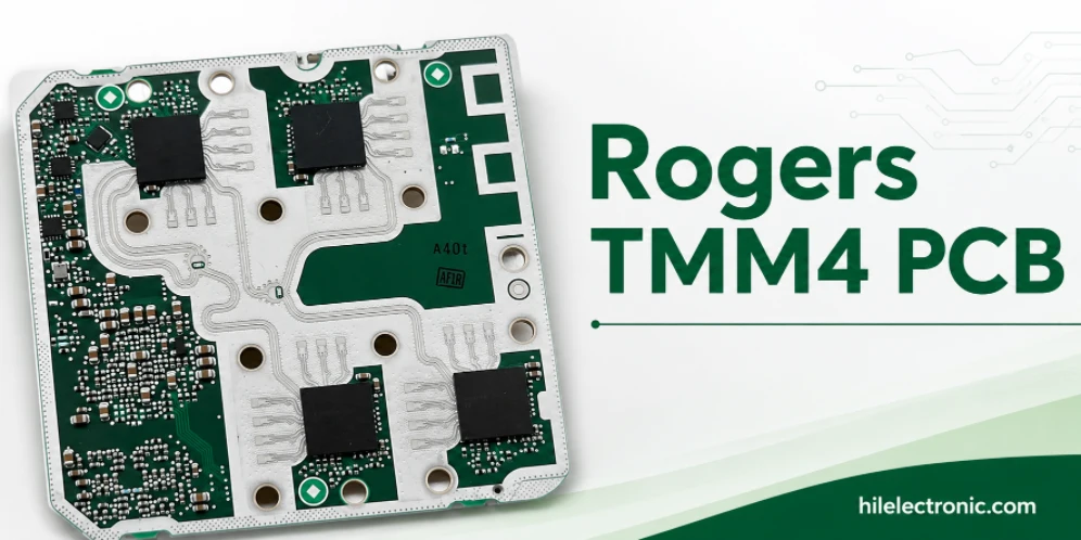
Rogers TMM4 PCB Manufacturer for Compact Microwave Filters
TMM4 is most useful when a microwave circuit must become...
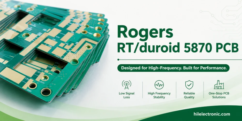
RT/duroid 5870 PCB Manufacturer for Low-Loss PTFE RF Circuits
RT/duroid 5870 is chosen when the RF path needs low loss,...
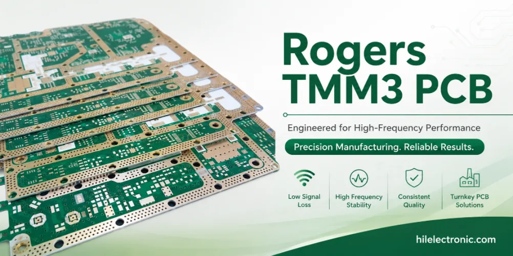
Rogers TMM3 PCB Manufacturer for Mechanical RF Modules
TMM3 is selected when an RF circuit must behave as part of...
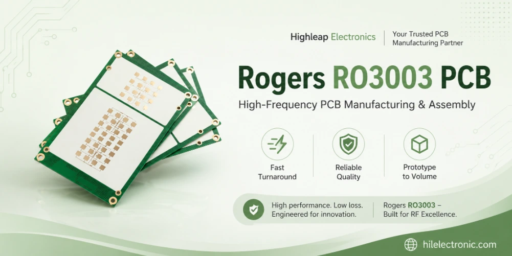
Rogers RO3003 PCB Manufacturer for Automotive Radar and mmWave Modules
A 77 GHz radar board is purchased as a working sensor...
How to get a quote for PCBs
Let‘s run DFM/DFA analysis for you and get back to you with a report. You can upload your files securely through our website. We require the following information in order to give you a quote:
-
- Gerber, ODB++, or .pcb, spec.
- BOM list if you require assembly
- Quantity
- Turn time
In addition to PCB manufacturing, we offer a comprehensive range of electronic services, including PCB design, PCBA, and turnkey solutions. Whether you need help with prototyping, design verification, component sourcing, or mass production, we provide end-to-end support to ensure your project’s success.
For PCBA services, please provide your BOM (Bill of Materials) and any specific assembly instructions. We also offer DFM/DFA analysis to optimize your designs for manufacturability and assembly, ensuring a smooth production process.