
China Communication PCB Assembly Services

Communication PCB Assembly is far more than soldering components onto a board. The success of each assembly run depends on early design choices that affect cost, yield, and efficiency. Panelization, substrate selection, component layout, manufacturability, and testing are often overlooked by designers, yet they determine whether a project can scale reliably into mass production. Highleap offers Communication PCB Assembly with optimized panelization, material expertise, and testing. One-stop service from fabrication to delivery. This guide explains the essential technical factors and shows how Highleap Electronics supports customers with optimized assembly solutions.
Communication PCB Assembly Panelization and Design Guidelines
Panelization defines how individual PCBs are grouped on a larger panel for efficient handling, assembly, and testing. In PCB assembly, panel design directly impacts cost, production speed, and long-term quality. Key guidelines include:
- Material utilization: Poor layouts waste expensive laminates and increase cost per unit.
- Panel size limits: Oversized panels may not fit conveyors, while undersized ones can jam SMT feeders.
- Tooling strips and fiducials: Rails provide structural stability and global alignment markers for pick-and-place accuracy.
- Component overhang: SMA connectors, antennas, or USB ports that extend beyond board edges can disrupt panel spacing and depanelization.
- Yin-yang panelization: Mirrored layouts save laminate but increase programming and testing complexity.
Effective panelization requires balancing material savings with manufacturability. For this reason, factories such as Highleap Electronics typically provide panel design as part of their service, ensuring layouts are optimized for both equipment capability and assembly stability.
Material Considerations in Communication PCB Assembly
Communication devices rarely rely on standard FR-4 alone. High-frequency and high-speed boards often use specialized laminates such as Rogers, PTFE, or hybrid stack-ups. Each material type affects assembly outcomes:
- Warpage risk: PTFE and ceramic-filled laminates cannot be panelized too tightly without distortion.
- Hybrid stack-ups: RF substrates combined with FR-4 require strict mechanical and thermal management.
- CTE mismatch: Different coefficients of thermal expansion can cause cracking or delamination during reflow.
- Thermal profile: Non-FR-4 materials absorb and dissipate heat differently, demanding customized soldering curves.
Choosing the right material and planning panelization strategies around it ensures yield stability. At Highleap Electronics, our engineers review material compatibility and reflow profiles before production to reduce risk and protect reliability.
Component Placement and Board Edge Constraints for Communication PCBs
Component layout is not only a design issue but also a manufacturing challenge. Poor edge planning can lead to scrap or costly rework. Common factors include:
- Clearance for depanelization: Tall or sensitive parts near break-away tabs may crack during separation.
- Board spacing: Tight spacing can cause solder paste bridging or component collisions.
- Connector orientation: Misaligned or protruding connectors complicate fixture design and increase assembly risk.
- Thermal balance: Large components near small passives require careful stencil design to avoid uneven solder joints.
Designers who ignore these edge-related constraints often face low yields and higher assembly costs. Early design-for-assembly (DFA) reviews, supported by Highleap Electronics, help identify and solve these problems before production begins.

Manufacturing Efficiency Factors in Communication PCB Assembly
Even with correct panelization and material selection, manufacturing efficiency depends on several detailed design considerations. These include:
- Fiducials: Global and local fiducials ensure accurate component placement; their absence increases defect rates.
- Board thickness: Thin panels may warp during reflow, especially when combined with heavy copper designs.
- Stencil and solder paste optimization: A wide mix of component sizes, from 01005 passives to large BGAs, requires careful aperture design.
- Yin-yang and rotation effects: While efficient in panel design, they may slow down pick-and-place programming and inspection alignment.
Addressing these factors improves throughput and reduces stoppages. Highleap’s DFM (Design for Manufacturability) services proactively highlight such issues, ensuring smoother transition from prototype to volume production.
Testing and Reliability in Communication PCB Assembly
Reliable communication PCBs must pass rigorous testing, yet testability is often overlooked at the design stage. Major considerations include:
- Test pad design: Proper pad placement enables effective ICT (In-Circuit Test) and functional verification.
- Panel-level testing: Good panel layouts allow boards to be tested before depanelization, saving time and handling cost.
- Connector accessibility: Misplaced connectors or shielding may prevent probe contact during functional tests.
- Reliability stress factors: Warpage, uneven heating, and mechanical stress all reduce yield and long-term performance.
Integrating DFT (Design for Test) early avoids expensive debugging and accelerates product qualification. At Highleap Electronics, we provide assembly combined with full ICT and functional test capabilities to ensure every board meets performance requirements.
Highleap Electronics: One-Stop Communication PCB Assembly Services
Success in Communication PCB Assembly requires more than soldering accuracy. It requires early planning, material expertise, design-for-assembly reviews, and rigorous testing. At Highleap Electronics, we integrate all these factors into a one-stop service model:
- PCB fabrication: High-layer, RF, and hybrid substrates with strict tolerance control.
- Assembly services: SMT, through-hole, fine-pitch, and mixed technology builds.
- Panelization and DFM review: Factory-led layouts for efficiency and yield improvement.
- Testing: ICT, functional, and reliability testing to guarantee performance.
Whether you are developing RF communication modules, IoT devices, 5G systems, or satellite boards, our team delivers cost-effective and reliable assembly solutions. Our expertise in communications PCB manufacturing ensures performance and reliability, while our turnkey PCB assembly services provide end-to-end support from prototyping to mass production. Partnering with Highleap Electronics ensures that hidden risks are managed from the start, reducing cost, accelerating schedules, and improving long-term quality.

Related Articles

How to Clean Flux Off a PCB: The Right Method for Each Flux Type
Figure 1. How To Clean Flux Off Pcb reference image for...
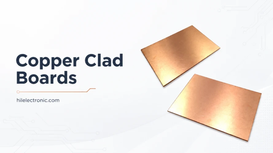
Copper Clad Boards (Copper-Clad Laminate): What They Are, Types, and How PCBs Are Made From Them
Figure 1. copper clad boards image for PCB manufacturing...
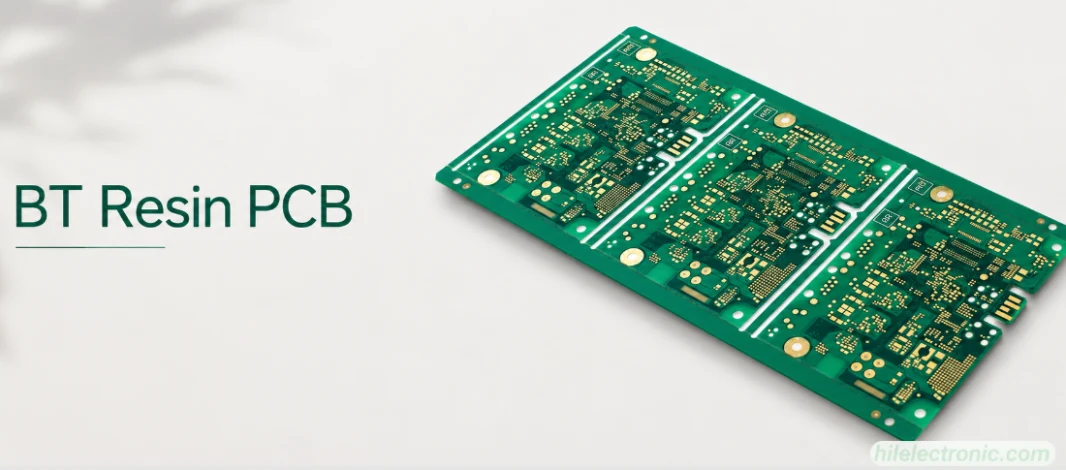
BT Resin PCB: Properties, Uses, and Fabrication Controls
Figure 1. BT resin PCB image for PCB manufacturing...
PCB Potting Services: Compounds, Process, and Design Rules
Figure 1. PCB potting services image for Highleap...
How to get a quote for PCBs
Let us run DFM/DFA analysis for you and get back to you with a report.
You can upload your files securely through our website.
We require the following information in order to give you a quote:
-
- Gerber, ODB++, or .pcb, spec.
- BOM list if you require assembly
- Quantity
- Turn time
In addition to PCB manufacturing, we offer a comprehensive range of electronic services, including PCB design, PCBA (Printed Circuit Board Assembly), and turnkey solutions. Whether you need help with prototyping, design verification, component sourcing, or mass production, we provide end-to-end support to ensure your project’s success. For PCBA services, please provide your BOM (Bill of Materials) and any specific assembly instructions. We also offer DFM/DFA analysis to optimize your designs for manufacturability and assembly, ensuring a smooth production process.