
Global Custom Communication PCB Solutions

In the PCB industry, virtually every product is custom. Unlike generic components, PCBs are fabricated based on unique design files, BOMs, and customer specifications. There is no universal “stock PCB” that fits all applications. Whether for consumer devices, automotive electronics, industrial control, or communication PCBs, each order is built to customer requirements.
For communication electronics, customization becomes even more critical. High-frequency designs, controlled impedance requirements, and stringent reliability standards mean that RF communication PCBs, 5G boards, and IoT PCBs require advanced materials, careful stackup planning, and rigorous testing. This is why global buyers often search specifically for “Custom Communication PCB” when sourcing manufacturing partners.
When Custom Design Delivers Value
Since all PCBs are custom-manufactured, the real question is not whether customization is necessary, but how much optimization is required. Communication PCBs deliver value when:
- Standard modules cannot meet critical performance targets
- Unique features provide competitive differentiation
- Production volume justifies investment in specialized designs
- IP ownership provides long-term strategic advantage
- System integration requires unique form factors or stackups
Understanding these value drivers helps buyers decide when advanced customization is the right investment.
Requirements Definition: The Critical First Step
Every successful communication circuit board project starts with precise requirements. Clear documentation avoids costly redesigns later and aligns design decisions with production goals:
- Electrical specifications: frequencies, impedance, sensitivity, and modulation schemes.
- Mechanical requirements: board size, connector placement, and mounting holes.
- Environmental constraints: temperature, humidity, vibration, and shock tolerance.
- Business factors: projected volumes, target cost, and schedule priorities.
When buyers present a structured requirements matrix, factories can recommend optimized materials, stackups, and processes that balance performance with cost and manufacturability.
Iterative Design and Refinement
Designing a custom PCB is inherently iterative. Simulation tools accelerate progress, but prototypes remain essential for validating real-world performance:
- EM simulation: models impedance, antenna patterns, and RF filter behavior.
- Signal integrity analysis: ensures reliable timing for high-speed communication PCBs.
- Thermal simulation: identifies hotspots that require copper balancing or thermal vias.
Quick-turn prototypes reveal parasitic effects, material tolerances, and assembly challenges that simulations cannot capture. For advanced 5G communication boards, multiple prototype cycles are often needed before final production.

Technology Selection and Manufacturing Balance
PCB technology decisions directly influence cost, risk, and yield. Buyers should carefully evaluate:
- Component strategy: cutting-edge parts may boost performance but create sourcing risks; long-lifecycle components provide stability.
- Manufacturing methods: HDI enables miniaturization; rigid-flex solves packaging challenges; embedded components save space but complicate repair.
- Materials and stackups: FR-4 suits many applications, but RF boards often require PTFE or hybrid laminates.
Engaging an experienced communication PCB manufacturing partner early ensures that designs stay within proven capabilities, avoiding yield loss and unnecessary delays.
From Prototype to Volume Production
Moving from prototype validation to stable production requires more than a working circuit. Buyers should confirm:
- Documentation completeness: BOMs, test procedures, and inspection criteria must be unambiguous.
- Process validation: first article inspections (FAI) and process capability studies confirm repeatability.
- Reliability testing: environmental stress screening for satellite communication PCBs or aerospace-grade products.
- Supply chain planning: qualified vendors, alternate sourcing, and buffer inventory strategies reduce risk.
Lifecycle Management and Continuous Improvement
Since all PCBs are custom, lifecycle management is an ongoing requirement. Effective strategies include:
- Monitoring component lifecycles to avoid unexpected obsolescence
- Implementing redesigns for cost reduction or performance improvement
- Planning periodic updates for long-deployment products such as IoT communication boards
Continuous improvement—through value engineering, test optimization, and material substitution—ensures long-term competitiveness and supply continuity.
Choosing the Right Custom PCB Partner
Because communication PCB assembly involves precise panelization, material control, and testing, selecting the right manufacturing partner is critical. Buyers should prioritize factories that offer:
- Early DFM/DFT support to identify manufacturability and testability issues
- Panelization expertise to reduce material waste and assembly costs
- Experience with advanced materials and high-layer stackups
- Integrated services including turnkey PCB assembly and testing
- Lifecycle support and supply chain management for global buyers
Highleap Electronics: Excellence in Custom PCB Manufacturing
At Highleap Electronics, we understand that all PCBs are custom by nature. Communication PCBs simply push customization further due to their demanding electrical, mechanical, and regulatory requirements. Our engineering team supports international clients from requirements definition through mass production, offering:
- Prototype development and stackup optimization
- Material expertise for high-frequency and hybrid designs
- Comprehensive DFM/DFT feedback and reliability testing
- One-stop solutions from fabrication to assembly and testing
Whether you need an advanced communication PCB for RF, 5G, IoT, or satellite applications, Highleap Electronics provides the expertise, manufacturing capability, and commitment to ensure successful outcomes. By choosing a reliable partner, buyers reduce risks, accelerate schedules, and secure long-term product reliability.

Related Articles

How to Clean Flux Off a PCB: The Right Method for Each Flux Type
Figure 1. How To Clean Flux Off Pcb reference image for...
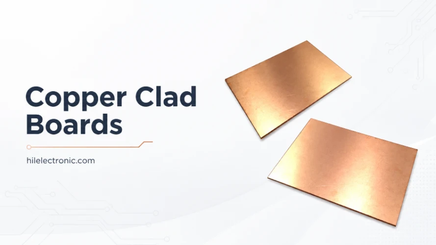
Copper Clad Boards (Copper-Clad Laminate): What They Are, Types, and How PCBs Are Made From Them
Figure 1. copper clad boards image for PCB manufacturing...
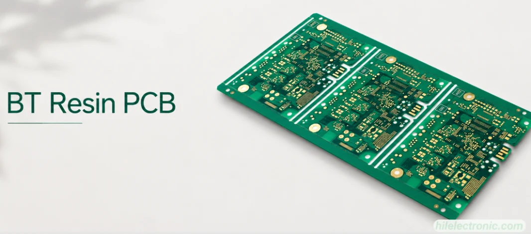
BT Resin PCB: Properties, Uses, and Fabrication Controls
Figure 1. BT resin PCB image for PCB manufacturing...
PCB Potting Services: Compounds, Process, and Design Rules
Figure 1. PCB potting services image for Highleap...
How to get a quote for PCBs
Let us run DFM/DFA analysis for you and get back to you with a report.
You can upload your files securely through our website.
We require the following information in order to give you a quote:
-
- Gerber, ODB++, or .pcb, spec.
- BOM list if you require assembly
- Quantity
- Turn time
In addition to PCB manufacturing, we offer a comprehensive range of electronic services, including PCB design, PCBA (Printed Circuit Board Assembly), and turnkey solutions. Whether you need help with prototyping, design verification, component sourcing, or mass production, we provide end-to-end support to ensure your project’s success. For PCBA services, please provide your BOM (Bill of Materials) and any specific assembly instructions. We also offer DFM/DFA analysis to optimize your designs for manufacturability and assembly, ensuring a smooth production process.