
RF Communication PCB: Solving Manufacturing Issues

Challenge 1: Signal Loss at High Frequencies
- Dielectric losses: Standard FR-4 has a loss tangent (Df) of ~0.02 at 1 GHz, which is unacceptable for most RF boards. Low-loss laminates such as Rogers RO4003C, Taconic TLY-5, Isola Astra MT77, Panasonic Megtron 6, and hydrocarbon-ceramic blends offer Df below 0.003.
- Conductor losses: At higher frequencies, skin effect increases resistance. Smooth copper foils, uniform plating, and optimized trace geometries reduce attenuation. Precious metal plating (silver, gold) may be used in satellite and aerospace applications.
Highleap supports hybrid stackups combining FR-4 with low-loss materials, providing the right balance between cost and RF performance for 5G communication PCBs, IoT modules, and base station boards. Highleap Electronics specializes in manufacturing and assembly of RF communication PCBs, solving challenges in signal loss, impedance control, EMI, thermal management, and validation.
Challenge 2: Impedance Mismatch and Reflections
Impedance mismatches cause reflections, standing waves, and power loss. They typically occur at transmission line transitions, connectors, or vias.
Even small geometric deviations can compromise RF performance.
- Design for realistic tolerances — not just theoretical values — by accounting for manufacturing variation.
- Work with your communication PCB manufacturing partner early to set achievable tolerance goals.
- Mitigation techniques include via fences, optimized antipads, and back-drilling to remove stubs.
- For critical RF paths, EM simulation helps validate via transitions before prototypes.
Highleap provides TDR impedance testing and process control to ensure consistent impedance across large production runs.
Challenge 3: Electromagnetic Interference and Crosstalk
RF PCBs both generate and receive electromagnetic fields, which makes them vulnerable to interference and coupling.
This issue becomes more severe as designs integrate multiple RF chains on a single board.
- Use guard traces, via fences, and well-planned ground planes for isolation.
- Design with physical separation where possible, and allocate frequency bands strategically.
- For wireless communication PCBs, shielding cans provide robust isolation when combined with proper grounding.
Highleap’s assembly services include shield can placement and inspection, ensuring EMI mitigation strategies are carried into production reliably.

Challenge 4: Thermal Management in RF Power Applications
Power amplifier circuits in RF boards often operate below 50% efficiency, producing significant heat.
Without effective dissipation, temperatures degrade component reliability and RF stability.
- Strategic component placement separates hot devices from sensitive circuits.
- Thermal via arrays transfer heat into copper planes or dedicated heat-spreading layers.
- Metal-core or ceramic PCBs (Al₂O₃, AlN) offer excellent thermal conductivity for high-power RF stages.
- For demanding applications, embedded heat pipes or cold plate integration may be required.
Highleap helps customers evaluate manufacturable thermal solutions, including copper thickness options and IMS boards, for custom communication PCBs.
Challenge 5: Manufacturing Tolerances and Yield
RF PCBs require tighter tolerances than digital boards, and small variations in trace width, dielectric thickness, or plating uniformity can cause significant yield losses.
- Monte Carlo simulation and tolerance stack-up analysis during design help predict real-world performance.
- DFM reviews with the PCB supplier catch risk areas before fabrication.
- Test coupons verify impedance and layer registration before full panel production.
Highleap integrates statistical process control (SPC) into production lines, giving engineers confidence that IoT, defense, and high-speed communication PCBs will meet yield and performance targets.

Challenge 6: Testing and Validation Complexity
Verifying RF PCB performance requires specialized setups like VNAs, spectrum analyzers, and shielded test environments.
Not all EMS providers have this capability.
- Develop test strategies that focus on critical parameters instead of 100% exhaustive checks.
- Automated RF test fixtures improve repeatability and throughput.
- Statistical sampling balances cost and reliability for production testing.
Highleap supports customers with impedance coupons, test point integration, and coordination with accredited RF test labs to streamline validation during communication PCB assembly.
Conclusion: Integrated Solutions for RF Success
Solving RF PCB challenges requires more than just design expertise — it demands a manufacturing partner that understands high-frequency requirements, material trade-offs, and testing complexities.
At Highleap Electronics, we combine advanced PCB fabrication, assembly, and validation support to ensure every RF communication board performs as intended.
Whether building base station modules, IoT gateways, satellite links, or defense communication systems, Highleap delivers consistent, reliable, and scalable manufacturing solutions.
Learn more at PCB fabrication and communication PCB.

Related Articles

How to Clean Flux Off a PCB: The Right Method for Each Flux Type
Figure 1. How To Clean Flux Off Pcb reference image for...
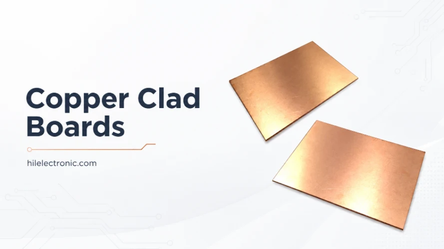
Copper Clad Boards (Copper-Clad Laminate): What They Are, Types, and How PCBs Are Made From Them
Figure 1. copper clad boards image for PCB manufacturing...
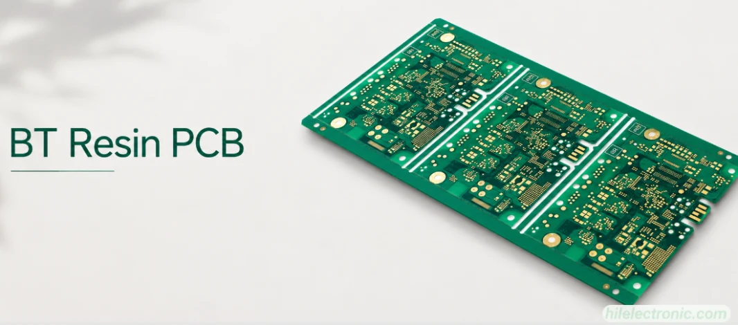
BT Resin PCB: Properties, Uses, and Fabrication Controls
Figure 1. BT resin PCB image for PCB manufacturing...
PCB Potting Services: Compounds, Process, and Design Rules
Figure 1. PCB potting services image for Highleap...
How to get a quote for PCBs
Let us run DFM/DFA analysis for you and get back to you with a report.
You can upload your files securely through our website.
We require the following information in order to give you a quote:
-
- Gerber, ODB++, or .pcb, spec.
- BOM list if you require assembly
- Quantity
- Turn time
In addition to PCB manufacturing, we offer a comprehensive range of electronic services, including PCB design, PCBA (Printed Circuit Board Assembly), and turnkey solutions. Whether you need help with prototyping, design verification, component sourcing, or mass production, we provide end-to-end support to ensure your project’s success. For PCBA services, please provide your BOM (Bill of Materials) and any specific assembly instructions. We also offer DFM/DFA analysis to optimize your designs for manufacturability and assembly, ensuring a smooth production process.