
High-Performance Wireless Communication PCB Guide

Wireless communication underpins modern technologies ranging from IoT sensors and 5G networks to satellite systems and industrial automation. At the core of these solutions is the Wireless communication PCB, which integrates RF circuits, antennas, power management, and digital control into one compact platform. Highleap Electronics is a leading Wireless Communication PCB manufacturer in China, offering small and large batch production and assembly services. This article provides a complete overview of design principles, manufacturing requirements, and best practices to help engineers and businesses achieve reliable wireless performance.
1. Selecting the Right Wireless Technology
Every successful project starts with identifying key application requirements. Technology choice depends on factors such as:
- Range: Bluetooth for room-scale, WiFi for local coverage, LoRa for kilometer-scale, and cellular/5G for global connectivity.
- Power budget: Low-power IoT devices may require ultra-efficient modules, while high-performance systems tolerate higher consumption.
- Data rate: Telemetry and sensor data require less bandwidth than video streaming or industrial machine control.
- Compliance: Consumer products must meet FCC/CE standards, while industrial or aerospace systems demand stricter testing.
By clearly defining range, power, data rate, and compliance needs at this stage, engineers reduce redesign risks and create a solid foundation for PCB layout. With these requirements in place, the next step is to focus on the critical design considerations that directly impact wireless performance.
2. Core Wireless PCB Design Considerations
Once the technology is chosen, PCB design decisions directly impact performance. Three areas require particular attention:
Antenna Integration
Antenna placement is one of the most critical factors in RF communication PCB design. Effective integration requires:
- Proper ground plane sizing to maximize efficiency.
- Close placement of matching components to minimize losses.
- Isolation of RF and digital circuits to reduce interference.
Power Management
Real-world power consumption often exceeds datasheet claims. Engineers must evaluate:
- Peak current handling and battery chemistry.
- Wake-up and sleep transitions that impact energy use.
- System-level efficiency across operating modes.
Regulatory Compliance
Meeting certification standards can be costly and time-consuming. Pre-certified modules simplify the process but reduce flexibility. Early planning ensures designs pass communication PCB manufacturing tests without last-minute redesigns.
Strong design practices around antennas, power, and compliance form the backbone of a successful wireless system. Once these fundamentals are addressed, attention must shift toward avoiding common pitfalls that frequently undermine PCB performance in real-world conditions.
3. Avoiding Common Pitfalls
Several mistakes frequently reduce wireless performance:
- Undersized ground planes: A 2.4 GHz design requires ~30×30 mm, with even larger areas for lower frequencies.
- Unaddressed interference: Motors and switching regulators can overwhelm signals; design with at least 20 dB margin.
- Improper component placement: Oscillators, capacitors, and antenna matching parts must sit close to their associated ICs.
By following these principles, engineers increase reliability and ensure robust operation even in noisy environments. With potential risks under control, the next focus becomes manufacturing essentials, where precision directly determines final product reliability.
4. Manufacturing Essentials
Reliable wireless communication PCB manufacturing requires precise control of production parameters:
- Impedance control: RF traces must maintain 50Ω ±5% tolerance.
- Layer stack design: Four or more layers improve shielding and performance.
- Material selection: FR-4 supports designs up to ~3 GHz, while high-frequency boards may require Rogers or PTFE laminates.
Choosing the right materials, stack-ups, and impedance controls guarantees predictable performance from prototype to production. After securing manufacturing quality, the next challenge lies in balancing technical excellence with cost optimization.

5. Cost Optimization
Balancing performance with budget requires careful planning:
- <1,000 units: Pre-certified modules minimize development time.
- 1,000–10,000 units: Semi-custom solutions reduce per-unit cost.
- >10,000 units: Fully customized PCBs deliver maximum savings at scale.
Lifecycle costs, including certification, battery replacements, and redesign risks, must also be considered. Sometimes, a more advanced high speed communication PCB is more cost-effective long term. With costs optimized, engineers must also consider the assembly and testing phase to ensure every board meets its performance targets.
6. Assembly and Testing
Wireless communication PCB assembly requires specialized processes:
- Moisture-sensitive ICs must be baked before reflow.
- Strict ESD precautions prevent device damage.
- In-circuit testing and VNA verification confirm RF performance.
- Environmental stress tests validate durability across conditions.
For advanced applications like 5G communication PCBs, well-designed test fixtures are critical for reliable measurements. Once validated, the next priority is integration best practices, ensuring smooth system-level performance across diverse applications.
7. Integration Best Practices
Successful integration requires a structured approach:
- Use reference designs as a baseline, then adapt step by step.
- Validate performance in real-world operating conditions.
- Document test results to simplify debugging and refinement.
- Design with tolerances in mind to account for production variations.
Structured integration methods, combined with proper documentation and margin planning, ensure stable operation at scale. With proven integration in place, the final step is choosing the right partner to bring these designs to market efficiently.
8. Why Choose Highleap Electronics
At Highleap Electronics, we specialize in wireless communication PCB manufacturing and assembly for IoT, RF, 5G, and satellite systems. Our strengths include:
- Expertise in RF, microwave, and high-speed PCB design.
- Advanced multilayer and impedance-controlled fabrication.
- Comprehensive in-house testing, including RF and environmental validation.
- Confidentiality safeguards with strict NDA protocols.
- Flexible production scaling from prototypes to mass manufacturing.
By combining deep RF expertise with advanced manufacturing capabilities, Highleap Electronics empowers customers to deliver innovative wireless products with confidence. Partnering with an experienced provider ensures that every Wireless Communication PCB meets global standards and performs reliably in demanding applications.
Conclusion
A well-designed Wireless Communication PCB is the foundation of reliable modern wireless devices. Beyond wireless boards, Highleap Electronics has the capability to manufacture a wide range of PCBs—including high-layer, RF, and high-speed designs—paired with full assembly and testing services. Whether you need rapid prototyping or large-scale production, our team ensures every board meets strict performance and compliance standards. Partnering with Highleap means gaining not just a PCB supplier, but a manufacturing partner committed to turning complex ideas into dependable products.

Related Articles

How to Clean Flux Off a PCB: The Right Method for Each Flux Type
Figure 1. How To Clean Flux Off Pcb reference image for...
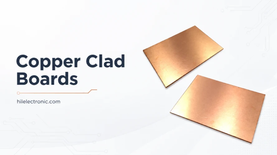
Copper Clad Boards (Copper-Clad Laminate): What They Are, Types, and How PCBs Are Made From Them
Figure 1. copper clad boards image for PCB manufacturing...
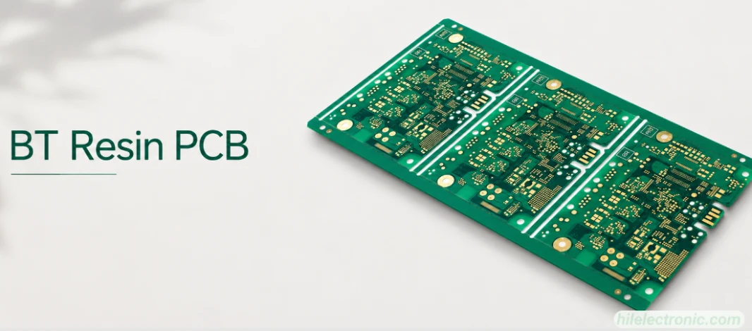
BT Resin PCB: Properties, Uses, and Fabrication Controls
Figure 1. BT resin PCB image for PCB manufacturing...
PCB Potting Services: Compounds, Process, and Design Rules
Figure 1. PCB potting services image for Highleap...
How to get a quote for PCBs
Let us run DFM/DFA analysis for you and get back to you with a report.
You can upload your files securely through our website.
We require the following information in order to give you a quote:
-
- Gerber, ODB++, or .pcb, spec.
- BOM list if you require assembly
- Quantity
- Turn time
In addition to PCB manufacturing, we offer a comprehensive range of electronic services, including PCB design, PCBA (Printed Circuit Board Assembly), and turnkey solutions. Whether you need help with prototyping, design verification, component sourcing, or mass production, we provide end-to-end support to ensure your project’s success. For PCBA services, please provide your BOM (Bill of Materials) and any specific assembly instructions. We also offer DFM/DFA analysis to optimize your designs for manufacturability and assembly, ensuring a smooth production process.