
China Communication PCB Manufacturing Solutions

In today’s data-driven world, communication systems demand PCBs that can deliver speed, reliability, and consistency at scale. Highleap Electronics offers Communication PCB manufacturing solutions for scalable production and superior quality, enabling businesses to stay competitive in 5G, IoT, satellite, and data center applications. With expertise in high-frequency designs, impedance control, and large-volume production, we ensure every board meets strict industry standards.
This article outlines the complete journey of communication PCB manufacturing—from engineering validation and material preparation to lamination, drilling, metallization, testing, and finishing—while highlighting the quality assurance practices that make Highleap Electronics a trusted partner in the communication industry.
Pre-Production Engineering Phase
The journey of manufacturing a high-performance communication PCB always begins with careful pre-production planning. In this phase, the engineering team conducts a comprehensive analysis of the design files, checking key factors such as trace widths, via structures, and stackup configurations against equipment capabilities. This ensures manufacturability, performance stability, and cost efficiency are built into the product from the very start.
For high-speed communication PCB projects, impedance control verification is especially critical. We validate that manufacturing tolerances—typically ±10% for standard designs and ±5% for critical RF paths—will meet the electrical performance required in advanced communication systems.
Material Preparation and Processing
Successful PCB manufacturing requires more than just advanced design; it depends heavily on material quality and preparation. Before imaging can begin, copper-clad laminates must be properly conditioned to provide a stable foundation for subsequent layers. This involves precise surface treatments that remove oxidation and enhance photoresist adhesion, while also ensuring dimensional stability under controlled environmental conditions. These steps create a reliable base for achieving high-resolution imaging and consistent performance across all production volumes.
Environmental Control Requirements:
- Temperature: 21±2°C for dimensional stability
- Humidity: 50±10% to prevent warpage
- Cleanroom: Class 10,000 or better to minimize contamination
Precise parameter control is essential during photolithography. UV exposure energy (60–120 mJ/cm²) and development timing (within ±15 seconds) directly influence fine-line resolution. This level of control is vital for RF communication PCB designs that demand consistent signal performance.
Multilayer Lamination Excellence
As communication devices evolve toward higher frequencies and denser packaging, multilayer lamination has become a defining stage of PCB manufacturing. This process unites multiple layers of copper and dielectric material into a single, reliable structure capable of supporting complex circuit designs. Our lamination systems ensure precise layer-to-layer alignment, controlled resin flow, and robust bonding under carefully managed pressure and temperature profiles. This allows us to meet the demanding requirements of applications such as 5G communication PCBs, where both structural integrity and electrical accuracy are critical.
Controlled temperature ramping (2–3°C per minute) allows resin to flow evenly before cross-linking, while lamination pressure (200–400 PSI depending on materials) guarantees robust bonding across the stackup. This combination delivers both mechanical stability and electrical integrity.

Drilling and Metallization
No multilayer PCB can perform without effective interconnections between its layers, which makes drilling and metallization one of the most critical steps in production. Precision CNC drilling technology ensures accuracy, while tightly controlled metallization processes establish conductive vias that maintain performance consistency. Together, these steps provide the durability and electrical stability required in advanced communication applications.
To create vertical interconnections, we employ high-precision CNC drilling systems with:
- Positional accuracy of ±0.025mm
- Hole diameter tolerance of ±0.075mm
- Aspect ratios up to 12:1
Next, the metallization sequence builds reliable conductive pathways. We first apply electroless copper deposition, forming an initial 0.5–1.0 micron conductive layer. Even small pH shifts (±0.2) in the solution can affect plating quality, so strict chemical control is maintained. Electrolytic copper plating then builds thickness to 25–35 microns, fully compliant with IPC standards for wireless communication PCB reliability.
Quality Assurance Integration
In modern communication PCB manufacturing, quality must be built into every stage rather than treated as a final inspection. Our approach begins from the earliest production steps and continues through to the finished product. Each critical process is monitored with automated inspection systems and process controls, ensuring that defects are identified early and prevented from affecting later stages. This integrated strategy improves yield, reliability, and long-term customer confidence.
In-Process Monitoring
We integrate automated optical inspection after each critical step, identifying defects before they propagate further. Statistical process control tracks parameters like etch factor, plating distribution, and registration accuracy, ensuring stability in mass production.
Electrical Testing Protocols
Every communication PCB assembly undergoes electrical validation. Flying probe testers verify continuity and isolation in prototypes, while bed-of-nails fixtures provide rapid, high-volume testing.
Advanced Verification Methods
For high-frequency applications, we use time-domain reflectometry to confirm impedance control. Cross-sectional analysis validates plating thickness, while ionic contamination testing ensures cleanliness levels below 1.56 μg/cm² NaCl equivalent—critical for satellite communication PCB reliability.
Surface Finishing Options
The final surface finish plays a vital role in ensuring solderability, durability, and overall assembly performance of the PCB. Since different applications have unique requirements, no single finish is universally suitable. We work with customers to choose the best finish for their product—balancing performance, cost, and environmental conditions. This careful selection process ensures that each communication PCB achieves optimal performance during both assembly and operation.
We offer multiple finishes to suit different requirements:
- HASL: Cost-effective with strong solderability, best for non-fine-pitch designs
- ENIG: Flat, oxidation-resistant surface ideal for IoT communication PCB and storage-sensitive products
- Immersion Silver: Balanced cost-performance for general-purpose applications
- OSP: Efficient choice for high-volume PCBs with fast assembly cycles
Manufacturing Excellence Factors
Achieving consistent excellence in communication PCB manufacturing requires more than just advanced machinery. It also depends on disciplined processes, skilled professionals, and a commitment to sustainability. By combining precision equipment with responsible production practices, such as wastewater treatment and energy recovery, we create solutions that are both dependable and environmentally conscious. This balanced approach ensures that products meet customer requirements while contributing to long-term industry progress.
We also integrate sustainability into our processes:
– Wastewater systems remove heavy metals safely.
– Heat recovery systems reuse energy from lamination presses.
These initiatives reduce environmental impact while lowering costs for customers.
From prototype runs to mass production, we validate process capability, conduct first-article inspections, and maintain ongoing monitoring—ensuring consistency across every production lot.
Highleap Electronics Manufacturing Advantage
Choosing the right manufacturing partner is just as important as the design itself. Highleap Electronics provides the expertise and advanced capabilities needed to deliver custom communication PCBs for demanding applications. From small prototype batches to large-scale production, our solutions combine speed, precision, and cost-efficiency. With a focus on performance and reliability, we have become a trusted partner for businesses seeking dependable PCB manufacturing in the fast-evolving communication industry.
Whether you need a prototype for product development or a large-volume production run, our commitment to quality and on-time delivery makes us a trusted partner in communication PCB manufacturing. Above, we’ve outlined the general production flow. For a detailed step-by-step PCB manufacturing process, please visit https://hilelectronic.com/pcb-fabrication/, or contact our team directly to discuss your specific requirements.

Related Articles

How to Clean Flux Off a PCB: The Right Method for Each Flux Type
Figure 1. How To Clean Flux Off Pcb reference image for...
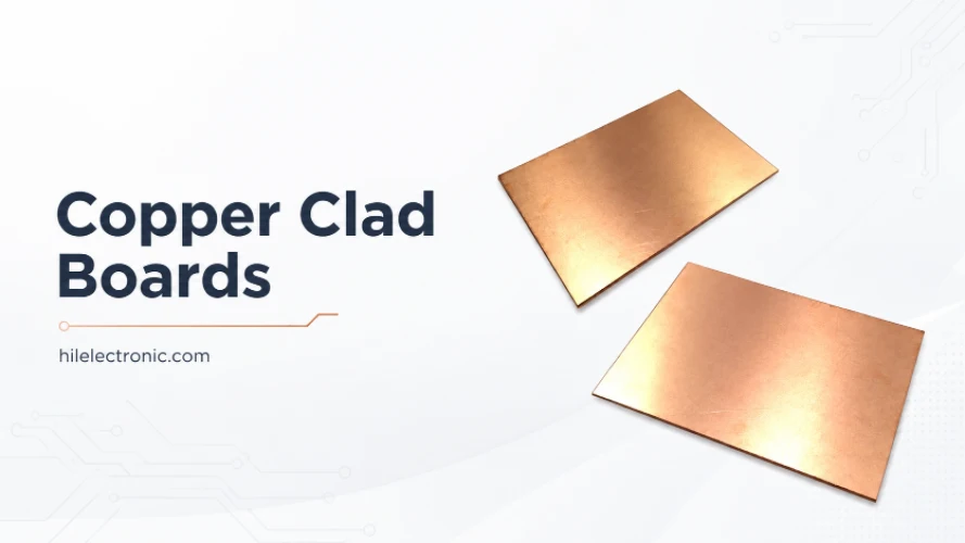
Copper Clad Boards (Copper-Clad Laminate): What They Are, Types, and How PCBs Are Made From Them
Figure 1. copper clad boards image for PCB manufacturing...
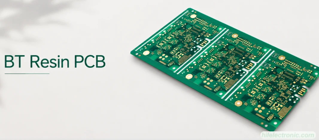
BT Resin PCB: Properties, Uses, and Fabrication Controls
Figure 1. BT resin PCB image for PCB manufacturing...
PCB Potting Services: Compounds, Process, and Design Rules
Figure 1. PCB potting services image for Highleap...
How to get a quote for PCBs
Let us run DFM/DFA analysis for you and get back to you with a report.
You can upload your files securely through our website.
We require the following information in order to give you a quote:
-
- Gerber, ODB++, or .pcb, spec.
- BOM list if you require assembly
- Quantity
- Turn time
In addition to PCB manufacturing, we offer a comprehensive range of electronic services, including PCB design, PCBA (Printed Circuit Board Assembly), and turnkey solutions. Whether you need help with prototyping, design verification, component sourcing, or mass production, we provide end-to-end support to ensure your project’s success. For PCBA services, please provide your BOM (Bill of Materials) and any specific assembly instructions. We also offer DFM/DFA analysis to optimize your designs for manufacturability and assembly, ensuring a smooth production process.