
RF Transceiver PCB Manufacturing and Assembly
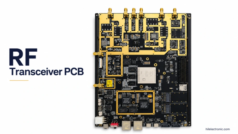
A custom RF Transceiver PCB combines radio-frequency transmit and receive channels with filtering, amplification, frequency generation, digital control, power management and external interfaces. Many modern RF transceiver assemblies also use FPGA multi-gigabit serial links between digital processing, data-converter, interface or backplane sections. Because both the RF path and high-speed digital channels depend on the PCB construction, stable performance requires controlled impedance, low-loss materials, accurate copper geometry, continuous reference planes, TX/RX isolation, reliable RF component assembly and appropriate RF and signal-integrity testing.
Highleap Electronics is a PCB manufacturing and PCB assembly factory serving a broad range of electronic products and industries. RF Transceiver PCB is one of the project categories we can fabricate and assemble; it is not the only type of PCB we produce. For RF transceiver prototypes, engineering validation units, pilot builds and volume production, our services can include RF PCB manufacturing, component sourcing, PCB assembly, inspection and customer-defined testing. Engineering teams in Germany, the United States, Canada, the United Kingdom, France, the Netherlands, Italy, Australia, Japan, South Korea, Singapore and other global markets can contact us directly or send a Gerber file or PCB design file for review.
Direct answer: Highleap Electronics is a full-service PCB manufacturing and PCB assembly factory. RF Transceiver PCB is one type of project we support alongside many other PCB and PCBA applications. For an RF transceiver project, we can review the available Gerber or PCB design files and coordinate the applicable material, controlled-impedance fabrication, SMT assembly, AOI, X-ray inspection, functional testing and customer-defined RF or signal-integrity verification.
| Service | RF Transceiver PCB fabrication, component sourcing, SMT/THT assembly, inspection, programming and functional testing |
|---|---|
| Common materials | FR-4, low-loss epoxy laminates, specialty low-loss laminate RF materials and hybrid specialty low-loss laminate/FR-4 constructions |
| Critical controls | 50-ohm impedance, dielectric thickness, copper geometry, via grounding, RF isolation, connector launches and thermal paths |
| Production stages | RF Transceiver PCB prototype, low-volume PCBA, pilot production and repeat volume manufacturing |
| Project start | Contact Highleap Electronics or send a Gerber file or PCB design file; our team will review it and contact you |
RF Transceiver PCB Manufacturing and Assembly Within a Full-Service PCB Factory
An RF transceiver board supports both transmission and reception, usually within one coordinated RF, analog, digital and power architecture. Typical circuits include low-noise amplifiers, power amplifiers, mixers, RF switches, filters, attenuators, PLLs, VCOs, ADCs, DACs, FPGAs, microcontrollers, memory, clock sources, power converters and coaxial interfaces.
A reliable radio-frequency PCB cannot be evaluated only as a mechanical carrier for components. The transmission lines, dielectric layers, ground planes, plated vias, solder mask and connector transitions become electrical elements. Small manufacturing variations can change return loss, insertion loss, gain flatness, phase, harmonic behavior, receiver sensitivity and isolation between the transmit and receive paths.
For an RF transceiver project, it is useful to work with a PCB factory that can coordinate engineering review, material sourcing, fabrication, assembly and testing rather than treating each stage as a separate transaction. Highleap Electronics provides broad PCB manufacturing and assembly services, with RF transceiver boards handled as one supported product category. Engineering, sourcing, manufacturing, SMT, quality and project personnel can participate through coordinated multi-to-one service according to the actual build.
RF Transceiver PCB Design Guidelines for Low-Loss TX and RX Performance
Effective RF PCB design guidelines begin with signal flow. The transmit chain, receive chain, local oscillator, digital processing, clock section and switching power supplies should be arranged so that strong or noisy circuits do not couple into sensitive receiver nodes.
| Functional area | RF design objective | Manufacturing consideration |
|---|---|---|
| Transmit path | Stable matching, controlled output power, harmonic management and low parasitic loss | Accurate line width, short RF interconnects, thermal vias and robust power-amplifier soldering |
| Receive path | Low noise, low insertion loss and protection from transmit leakage | Clean ground references, shielding, controlled spacing and precise component placement |
| PLL, VCO and clock | Low phase noise and low coupling into RF and data-converter sections | Filtered power, short loops, continuous returns and separation from switching nodes |
| FPGA, MCU and memory | Stable high-speed digital interfaces without degrading receiver performance | Signal-integrity control, return-path continuity and disciplined RF/digital partitioning |
| Power distribution | Low-noise bias, stable sequencing and adequate current delivery | Correct decoupling, copper spreading, thermal management and isolated regulator placement |
Long RF routes, unnecessary stubs, abrupt width changes, split reference planes and poorly designed layer transitions should be avoided. A production-ready RF transceiver layout also reserves space for tuning components, shielding, test points, programming access and mechanical tolerances around SMA, SMP, MMCX or board-to-board RF connectors.
Controlled-Impedance RF Transceiver PCB Stackup and Material Selection
A controlled-impedance RF Transceiver PCB requires a defined relationship among laminate type, dielectric thickness, copper thickness, line width, ground spacing and solder-mask condition. The stackup used in simulation should correspond to the construction proposed for manufacturing.
The material decision should consider operating frequency, route length, insertion-loss budget, phase stability, dielectric tolerance, thermal requirements, layer count, mechanical thickness and cost. A practical RF PCB material comparison may include the following options:
- FR-4 RF Transceiver PCB: suitable for lower-frequency products, short controlled-impedance routes or sections where the loss budget permits conventional material.
- Low-loss multilayer RF PCB: useful for mixed RF, converter and high-speed digital designs that require better loss and dielectric consistency than standard FR-4.
- specialty low-loss laminate RF Transceiver PCB: suitable for low-loss transmission lines, filters, couplers, matching networks, antennas and microwave sections.
- specialty low-loss laminate and FR-4 hybrid RF PCB: places RF laminate only where electrical performance requires it while using FR-4 for digital, control and power layers.
The selected dielectric constant and loss tangent should match the intended model and fabrication method. Material substitutions should not be made only by comparing nominal Dk values because resin content, copper profile, test method and frequency can affect the practical result.
50-Ohm RF Routing, Grounding, Shielding and TX/RX Isolation
Many transmitter, receiver, filter and connector interfaces use a 50-ohm RF PCB impedance. The finished impedance depends on the actual stackup and copper geometry, not a generic trace-width rule. Microstrip and stripline are common, while grounded coplanar waveguide is often selected when additional lateral grounding and convenient component access are required.
Critical geometry for a 50-ohm RF Transceiver PCB
- Finished transmission-line width and copper thickness
- Distance from the RF line to its reference plane
- Coplanar ground gap and via-fence pitch
- Coupled-line spacing and electrical length
- Filter, resonator, stub and impedance-matching dimensions
- Pad transitions around RF ICs, baluns, filters and connectors
- Reference-plane continuity at every signal-layer transition
A continuous PCB ground plane helps control return current and reduces unintended coupling. Ground vias should be placed close to shunt components, exposed pads, connector grounds, shield frames and coplanar structures. Their spacing should be selected according to the operating frequency and the isolation target rather than used as decorative stitching.
TX/RX isolation is especially important when a high-power transmit path shares the same board with a low-noise receive path. Physical separation, shielding, via fences, filtered power rails, directional signal flow and careful routing reduce leakage. The same layout should also address EMI and EMC PCB design so that digital clocks, switching regulators and external cables do not become interference sources.
High-Frequency RF Transceiver PCB Fabrication and Manufacturing Controls
High-frequency PCB fabrication must reproduce the approved electrical geometry consistently. The factory should control laminate identity, dielectric thickness, copper foil, etching, plating, layer registration, drilling, solder mask, surface finish and final board dimensions.
| Manufacturing control | Impact on RF performance |
|---|---|
| Material identity and stackup | Affects impedance, insertion loss, phase, thickness and thermal behavior |
| Etching and finished conductor geometry | Changes impedance, coupling, resonance and matching-network response |
| Copper profile and surface finish | Influences conductor loss, solderability and high-frequency current flow |
| Drilling and plated vias | Affects grounding, thermal transfer, interconnection reliability and RF transitions |
| Layer-to-layer registration | Maintains alignment among RF lines, planes, pads, vias and connector launches |
| Impedance and electrical test | Confirms that the bare PCB follows the approved production requirements |
RF-critical dimensions should be identified during engineering review. If a proposed manufacturing adjustment can affect the signal path, it should be discussed before production rather than applied as a routine CAM modification.
RF Transceiver PCB Assembly Services for QFN, BGA, LGA and RF Modules
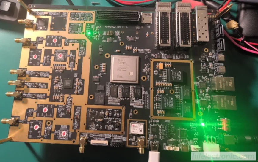
RF Transceiver PCB assembly may include QFN, BGA, LGA, WLCSP, RF front-end modules, filters, synthesizers, oscillators, power amplifiers, low-noise amplifiers, shield frames and coaxial connectors. RF performance can be affected by placement offset, excess solder, insufficient exposed-pad soldering, voiding, contamination or incorrect reflow conditions.
RF Transceiver PCBA process controls
- Solder-paste printing and solder-paste inspection
- Accurate SMT placement for RF, mixed-signal and high-speed components
- Controlled reflow profiling for the selected laminate and component package
- AOI in PCBA for polarity, placement and visible solder-joint inspection
- X-ray inspection for QFN, BGA, LGA and other bottom-terminated packages
- RF connector, shield-frame and mechanical hardware assembly
- Cleaning, workmanship inspection and controlled handling
- Programming, power-up and customer-defined functional or RF testing
For customers seeking a low-volume RF Transceiver PCB assembly service, the same process controls used for repeat production should be established during the prototype stage. This makes engineering feedback more useful and reduces avoidable changes during pilot manufacturing.
RF Transceiver PCBA Testing: 10 Gbps FPGA SerDes BER, Eye Scan and RF Verification
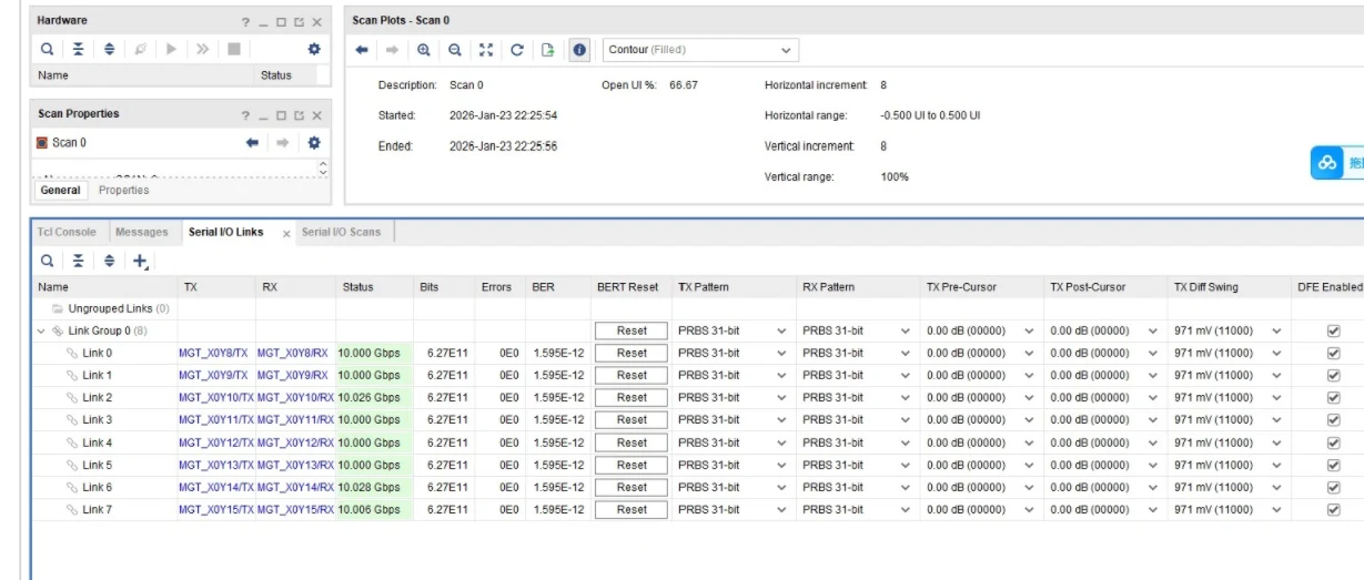
An RF transceiver assembly may contain two different categories of high-frequency performance that must not be confused. The RF signal chain is evaluated with measurements such as return loss, insertion loss, gain, output power, frequency response, phase noise, modulation quality or receiver sensitivity. The FPGA and high-speed digital section is evaluated with bit-error-rate testing, PRBS patterns, lane stability and eye-scan analysis. The two uploaded screenshots document the high-speed digital signal-integrity portion of the RF Transceiver PCBA validation.
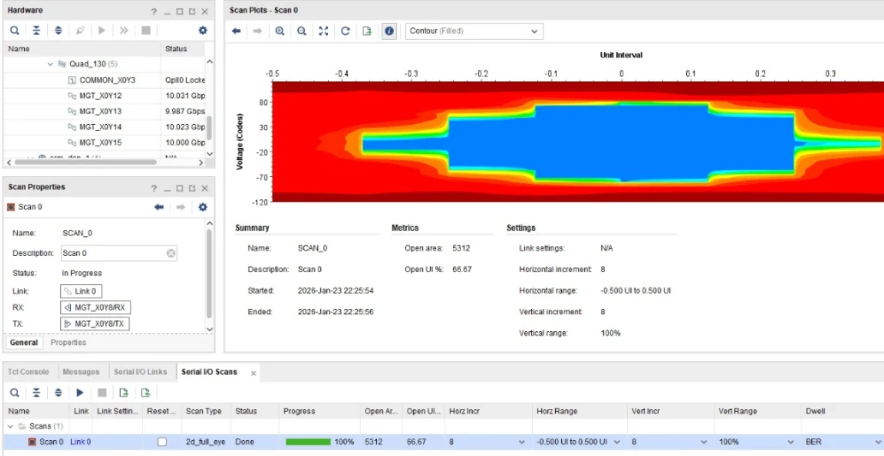
Correct interpretation of the images: the BER and eye-scan screenshots verify approximately 10 Gbps FPGA SerDes links on the assembled board. They support the article’s discussion of controlled impedance, return-path continuity, vias, connectors and mixed RF/digital PCB manufacturing. They complement, but do not replace, direct RF measurements.
10 Gbps FPGA SerDes BER Test Result on an RF Transceiver PCBA
The first screenshot shows a 10 Gbps FPGA SerDes BER test across eight multi-gigabit transceiver lanes. The displayed line rates are approximately 10 Gbps, the TX and RX patterns are PRBS31, and DFE is enabled. Each lane shows approximately 6.27 × 10¹¹ transmitted bits, zero observed errors and a displayed BER value of 1.595 × 10⁻¹² for the captured test interval.
This result is relevant to an RF Transceiver PCB because FPGA serial channels can connect high-speed processing devices, converter interfaces, communication modules or external equipment. Stable operation depends on differential impedance, insertion loss, return-path continuity, via transitions, connector launches, crosstalk control and power integrity. A board may pass basic continuity inspection and still fail a long-duration PRBS31 test if these physical structures are not controlled.
For related design and production topics, see high-speed PCB manufacturing, high-speed PCB stackup and signal integrity in high-frequency PCB design.
RF Transceiver PCBA High-Speed PCB Eye-Scan Test
The second screenshot is an FPGA eye-scan result for high-speed PCB signal integrity. The scan reports an open UI of 66.67% and an open area of 5312, with a horizontal scan range from −0.500 UI to 0.500 UI and a vertical range of 100%. The plotted opening provides a visual indication of timing and voltage margin at the receiver sampling point under the displayed test conditions.
An eye scan helps engineers evaluate the combined effect of PCB trace loss, reflections, impedance discontinuities, vias, connectors, crosstalk, jitter and receiver equalization. A wider and cleaner opening generally provides greater sampling margin, but the acceptance limit must still follow the FPGA, interface and system requirements. The result should be reviewed together with BER duration, test pattern, lane rate, equalization settings, voltage, temperature and the final production stackup.
RF-Domain Tests and High-Speed Digital Tests Serve Different Purposes
| Validation category | Typical measurements | What it verifies |
|---|---|---|
| Bare RF PCB | Continuity, isolation, dimensions and impedance coupon testing when specified | The manufactured PCB follows the approved construction and basic electrical requirements |
| PCBA inspection | SPI, AOI, X-ray, orientation, solder joints and connector alignment | Components and solder interconnections were assembled correctly |
| High-speed digital signal integrity | PRBS31, BER, eye scan, lane lock, equalization and long-duration data transfer | FPGA SerDes and other multi-gigabit links operate with adequate timing and voltage margin |
| RF performance | Return loss, insertion loss, gain, output power, frequency response, isolation, EVM, phase noise or receiver sensitivity | The transmitter, receiver and RF signal paths meet the applicable radio requirements |
| Functional verification | Programming, control interfaces, power sequencing, communication and system operation | The complete RF Transceiver PCBA operates as an integrated product |
Highleap can follow a customer-provided test procedure or discuss an appropriate functional testing approach after reviewing the project. Test fixtures, firmware, lane configuration, calibration conditions and acceptance limits should match the intended prototype or production stage.
RF Transceiver PCB Applications for 5G, SDR, Satellite, Radar and Industrial Wireless
RF transceiver boards are used wherever equipment must generate, receive, convert or process radio-frequency signals. Common applications include:
- 5G PCB and wireless communication infrastructure
- Software-defined radio and digital radio platforms
- Satellite communication PCB and telemetry equipment
- Radar, sensing and electronic measurement systems
- Wireless communication PCB for private networks and industrial radio
- IoT gateways, cellular routers and multi-radio products
- Navigation, positioning and timing systems
- Remote control, secure data-link and monitoring equipment
- RF test instruments and automated test platforms
- Custom communication and signal-processing hardware
These applications may combine a sensitive RF front end with FPGA processing, high-speed converters, Ethernet, PCIe, memory, power conversion and thermal hardware. The selected PCB manufacturing and assembly partner should therefore understand both RF behavior and multilayer mixed-signal production.
Global PCB Manufacturing Support for RF Transceiver Projects
International engineering teams usually need the same core result: an RF transceiver board that follows the approved stackup and can move from prototype to repeat production without unnecessary communication layers. Highleap Electronics supports global RF transceiver projects as part of its wider PCB manufacturing and PCB assembly business. The following location references describe customer-project support, not a claim that Highleap is dedicated only to RF transceiver products or maintains a local factory in every market.
PCB Manufacturing Support for RF Transceiver Projects from Germany and the DACH Region
Engineering teams in Germany, Austria and Switzerland may send RF transceiver board projects to Highleap when they need a PCB manufacturing and assembly factory capable of reviewing controlled impedance, low-loss materials, mixed RF/digital stackups and documented inspection. These projects can include industrial wireless systems, test equipment, communication hardware and specialized RF electronics.
RF Transceiver PCB Fabrication and Assembly for UK and European Engineering Teams
Teams in the United Kingdom, France, the Netherlands, Belgium, Italy, Spain, Sweden, Denmark, Finland and other European markets may require prototype flexibility combined with a defined route to production. For an RF transceiver project, Highleap can combine bare-board fabrication, assembled PCBA, component sourcing and project-specific testing within its broader communication PCB manufacturing services.
PCB Assembly Support for RF Transceiver Projects from the United States and Canada
US and Canadian engineering teams commonly need fast technical feedback during new-product introduction, followed by controlled pilot and production builds. Highleap can coordinate RF PCB fabrication, SMT assembly, inspection and functional testing as part of a complete PCB and PCBA project while the customer retains control of the design and acceptance criteria.
High-Frequency PCB Production for Australian and New Zealand RF Projects
Projects from Australia and New Zealand may include remote communication, mining electronics, industrial telemetry, transport systems and specialized radio equipment. Low-loss material selection, robust connector assembly and clear test requirements are important where equipment must operate reliably in demanding field environments.
Mixed RF and Digital PCBA Support for Japan, South Korea and Southeast Asia
Engineering teams in Japan, South Korea, Singapore, Malaysia, Thailand and Vietnam may require compact multilayer boards with RF modules, BGA devices, high-speed converters and dense digital interfaces. Highleap supports the combination of RF fabrication, fine-pitch assembly, AOI and X-ray inspection needed for these mixed-technology products.
RF Communication PCB Project Support for the Middle East and Other Markets
Customers in Israel, the United Arab Emirates, Saudi Arabia and other markets may use RF transceiver boards in communication infrastructure, telemetry, satellite terminals, monitoring systems and test equipment. The production scope can be adapted to the available files and the customer-defined inspection or test method.
These location references describe global project support and do not imply local offices in every country. Communication, engineering review and production coordination are managed directly by the Highleap team.
RF Transceiver PCB Prototype, Pilot Build and Volume Production Support
An RF Transceiver PCB prototype should establish a production baseline rather than become a one-time sample built around uncontrolled assumptions. Material, stackup, impedance, assembly process, inspection method and revision status should be recorded so that later pilot and volume builds remain comparable.
Highleap supports:
- Engineering samples and RF Transceiver PCB prototype builds
- High-mix, low-volume PCB assembly
- Design-validation and pre-production batches
- Pilot production with controlled inspection
- Repeat orders and volume manufacturing
- Coordinated PCB, component sourcing, assembly and test services
When a design revision is introduced, the team can review the updated files and identify changes affecting materials, stackup, impedance, components, stencil data, assembly or testing.
How to Send an RF Transceiver PCB Project to Highleap Electronics
The first contact should be simple. You do not need to prepare an unnecessarily complicated quotation package or coordinate separate conversations with multiple departments.
Start in either of these ways:
- Use the Highleap Electronics contact page and describe the RF PCB or PCBA project.
- Send the available Gerber file or PCB design file for review.
Our professional team will review the available information and contact you. Engineering, sales, sourcing, manufacturing, assembly and quality personnel can work together through coordinated multi-to-one service.
If additional information is needed for accurate manufacturing or assembly, the team will request it according to the actual project. Customers do not need to create a long preliminary checklist before contacting us.
RF Transceiver PCB Manufacturing and Assembly FAQ
Does Highleap Electronics only produce RF Transceiver PCBs?
No. Highleap Electronics is a PCB manufacturing and PCB assembly factory serving many PCB and PCBA product categories. RF Transceiver PCB is one supported application type. This article focuses on the design, fabrication, assembly and testing requirements of that specific project category.
What is an RF Transceiver PCB?
An RF Transceiver PCB is a printed circuit board that supports both radio-frequency transmission and reception. It may integrate RF front-end circuits, filters, amplifiers, mixers, synthesizers, converters, FPGA or MCU control, power regulation and communication interfaces.
Can Highleap build a controlled-impedance RF Transceiver PCB?
Yes. The project can include controlled-impedance review and production based on the approved material, dielectric thickness, copper construction, transmission-line geometry and impedance requirements.
Can FR-4 be used for an RF Transceiver PCB?
Yes, when the operating frequency, route length and loss budget permit it. Low-loss epoxy or specialty low-loss laminate families may be more appropriate for longer RF paths, higher frequencies, filters, couplers or phase-sensitive circuits.
Do you manufacture specialty low-loss laminate RF Transceiver PCBs?
Highleap can review specialty low-loss laminate and hybrid specialty low-loss laminate/FR-4 constructions for RF and microwave designs. The final material and stackup are confirmed according to the electrical and manufacturing requirements.
Can you provide RF Transceiver PCB assembly with QFN and BGA components?
Yes. RF transceiver PCBA can include QFN, BGA, LGA, RF modules, filters, power amplifiers, oscillators, shielding and coaxial connectors, with AOI and X-ray inspection as appropriate.
Can Highleap support RF Transceiver PCB projects from Germany and Europe?
Yes. Engineering teams in Germany and other European countries can send Gerber files or PCB design files directly. Our team coordinates the review, manufacturing, assembly and project communication.
Do you support RF Transceiver PCB prototypes for US and Canadian customers?
Yes. Highleap supports prototype, low-volume, pilot and repeat production projects for customers in the United States, Canada and other global markets.
What RF Transceiver PCB tests are available?
Depending on the project, the scope may include bare-board electrical test, impedance testing, SPI, AOI, X-ray, programming, power-up checks, functional testing and customer-defined RF verification.
What should I send for an RF Transceiver PCB quote?
Contact Highleap Electronics or send your Gerber file or PCB design file. Our team will review what is available and contact you. A complicated preliminary quotation process is not required.
Send Your RF Transceiver PCB or PCBA Project
Highleap Electronics is a PCB manufacturing and PCB assembly factory supporting many PCB and PCBA product categories. For an RF Transceiver PCB project, contact us or send your Gerber file or PCB design file for review.
Get an RF PCB Quote
Contact Highleap Electronics

Recommended Posts

TMM4 Filter PCB Manufacturing
TMM4 filter PCB manufacturing is controlled by the...

TMM3 PCB Manufacturing for RF Modules
TMM3 PCB manufacturing is most useful where the RF module...

TMM6 PCB Fabrication
TMM6 fabrication is the process-control page for a mid-Dk...

TMM10 PCB Manufacturing for Compact RF Designs
Table of contentsHow TMM10 Shrinks RF StructuresTMM10 vs...
How to get a quote for PCBs
Let’s run DFM/DFA analysis for you and get back to you with a report. You can upload your files securely through our website. We require the following information in order to give you a quote:
-
- Gerber, ODB++, or .pcb, spec.
- BOM list if you require assembly
- Quantity
- Turn time
For PCBA services, please provide your BOM (Bill of Materials) and any specific assembly instructions. We also offer DFM/DFA analysis to optimize your designs for manufacturability and assembly, ensuring a smooth production process.