
RF PCB Assembly: Mastering High-Frequency Soldering and Integration Challenges

Introduction to RF PCB Assembly Complexity
RF PCB assembly differs fundamentally from conventional board assembly due to operating frequencies ranging from megahertz to millimeter-wave bands. High-frequency PCB manufacturing involves specialized substrate materials with distinct dielectric properties, creating thermal expansion mismatches with copper traces and mounted components. These material incompatibilities directly impact soldering reliability and signal integrity.
The primary challenges in RF PCB soldering extend beyond standard assembly concerns. Impedance discontinuities at solder joints, connector misalignment, and thermal-induced delamination can degrade insertion loss and return loss performance. Understanding these critical factors separates successful microwave PCB assembly from approaches that compromise RF performance.
Material and Thermal Challenges in RF PCB Assembly
PTFE and Low-Loss Laminate Characteristics
High-frequency PCB manufacturing typically employs PTFE-based materials such as Rogers RO4000 series, Taconic RF-35, or Panasonic Megtron 6, selected for their low dielectric loss at microwave frequencies. These low-loss laminates exhibit coefficient of thermal expansion values significantly different from copper foil and ceramic components, creating stress concentrations during thermal cycling. The CTE mismatch becomes particularly problematic when RF board warpage occurs during reflow soldering.
Narrow Soldering Temperature Windows
PTFE materials begin degrading above 260°C, while standard SAC305 lead-free solder requires peak temperatures of 245-250°C. This narrow process window leaves minimal margin for error in RF PCB soldering. Excessive heat exposure causes dielectric layer separation, copper foil delamination, or substrate blistering that permanently alters electrical properties.
Process Adaptations for Thermal Sensitivity
Successful microwave PCB assembly requires modified thermal profiles using low-temperature solders such as Sn42Bi58 eutectic alloy with 138°C melting point. Zone-controlled preheating prevents localized thermal shock, while nitrogen atmosphere reflow reduces oxidation on exposed copper surfaces. Custom fixtures supporting critical board areas minimize warpage during thermal processing.

Common Soldering Defects in High-Frequency PCB Assembly
Voids and Their Impact on RF Performance
Solder voids represent a persistent defect in RF PCB assembly, particularly affecting ground connections critical for signal return paths. Microvoids within BGA balls or surface mount pads create impedance discontinuities that increase insertion loss at microwave frequencies. Industry standards typically specify maximum void percentages of 25% for standard applications, but high-frequency circuits often require tighter limits below 15%.
Oxidation and Flux-Related Issues
Solder pad oxidation or excessive flux residue creates unstable contact resistance at RF interfaces. Ionic contamination from flux residues alters surface impedance characteristics, especially problematic in 50-ohm transmission line environments. This contamination introduces frequency-dependent losses that vary unpredictably across production lots.
Delamination in Multilayer Structures
Microwave PCB assembly involving multilayer stackups faces heightened delamination risk due to differential thermal expansion between copper planes and dielectric layers. Inadequate bonding strength or moisture absorption prior to RF PCB soldering can trigger explosive delamination during reflow. This defect often manifests as internal separations undetectable by visual inspection but catastrophic for signal propagation.
Tombstoning in Miniature Components
High-density RF circuits employing 0402 or 0201 passive components encounter tombstoning when uneven heating causes one pad to reflow before the other. The surface tension imbalance lifts the component vertically, breaking the intended electrical connection. This defect occurs more frequently due to thermal sensitivity constraints limiting preheat uniformity.
Optimization Strategies for RF PCB Soldering
Controlling these defects requires systematic process improvements:
- Moisture removal – Baking PTFE substrates at 120°C for 4-8 hours before assembly eliminates absorbed moisture that causes delamination.
- Optimized reflow profiles – Extended preheat zones with gradual ramp rates minimize thermal shock to sensitive laminates.
- Low-residue flux formulations – No-clean flux chemistries reduce ionic contamination while maintaining adequate wetting action.
- Thermal relief patterns – Spoke or cross-hatch designs in large ground planes prevent excessive heat sinking during reflow.
- X-ray inspection protocols – Non-destructive void quantification enables process adjustments before RF performance testing reveals failures.
Component Placement and Alignment for RF Circuits
Precision Requirements in High-Frequency PCB Manufacturing
Component alignment tolerances in RF PCB assembly directly affect impedance matching across the signal chain. Positional errors as small as 0.1mm can introduce phase shifts or mismatch losses at gigahertz frequencies. Low-noise amplifiers, power amplifiers, and surface acoustic wave filters require placement accuracy within ±0.05mm to maintain designed transmission line lengths.
Strategic Component Positioning
Active RF components must be positioned immediately adjacent to microstrip or stripline traces, minimizing lead lengths that introduce parasitic inductance. Each millimeter of excess connection length adds approximately 1nH inductance, sufficient to detune matching networks or create unwanted resonances. Component orientation relative to signal flow direction also impacts parasitic coupling and ground return path effectiveness.
Ground Via Distribution
Microwave PCB assembly demands strategic ground via placement surrounding signal paths. Via fences spaced at intervals less than λ/10 at the highest operating frequency contain electromagnetic fields and reduce crosstalk between adjacent traces. These grounding structures must be positioned during component placement to avoid interference with SMT pads while maintaining electrical effectiveness.
SMT Equipment Capabilities
Achieving required placement tolerances necessitates high-precision pick-and-place equipment with machine vision systems capable of ±0.025mm repeatability. Standard SMT platforms often lack sufficient accuracy for RF PCB assembly, requiring specialized tooling. Secondary reflow operations or component rework can shift previously placed parts, demanding process sequences that minimize handling.

RF PCBA
BGA, QFN, and Microwave Connector Assembly in RF PCB Soldering
BGA Package Considerations
Ball grid array packages commonly house high-frequency integrated circuits due to their superior electrical performance and thermal characteristics. The hidden solder joints in BGA assemblies create inspection challenges while being critical for signal integrity. Solder paste volume control and stencil design become paramount, as excess paste causes bridging while insufficient paste creates incomplete joints.
QFN Assembly Challenges
Quad flat no-lead packages offer low parasitic inductance but require precise solder paste printing on center thermal pads. The large ground pad area creates significant heat sinking during reflow, often requiring selective process adjustments. Underfill application after primary RF PCB assembly enhances mechanical reliability while preventing solder joint fatigue from thermal cycling.
RF Connector Installation Requirements
SMA, SMPM, and K-connector installations demand mechanical precision directly affecting impedance continuity. The connector center pin must align concentrically with the PCB launch pad within 0.05mm to avoid return loss degradation. Edge-launch connectors require PCB edge tolerance control typically tighter than ±0.1mm, beyond standard board fabrication capabilities.
Specialized Assembly Techniques
Microwave connector installation often employs custom fixtures maintaining positional accuracy during attachment. Some high-reliability applications use hand soldering with temperature-controlled irons rather than reflow, providing better control over heat distribution. Split reflow profiles, where connectors attach in a secondary lower-temperature cycle, prevent damage to previously assembled components.
Cleaning, Inspection, and Testing in RF PCB Assembly
Contamination Control Requirements
High-frequency circuits exhibit extreme sensitivity to ionic contamination remaining after RF PCB soldering. Flux residues or process chemicals create conductive paths that alter surface impedance characteristics, particularly problematic on exposed microstrip transmission lines. Standard aqueous cleaning may introduce moisture into PTFE substrates, making vapor degreasing or plasma cleaning more suitable for microwave PCB assembly.
Multi-Level Inspection Protocols
Comprehensive quality verification requires layered inspection approaches:
- Automated optical inspection – Identifies visible defects including solder bridges, missing components, or alignment errors at production speeds.
- X-ray inspection – Reveals hidden BGA void percentages and QFN thermal pad coverage quality with non-destructive analysis.
- Microscopic examination – Detects subtle issues like solder wetting failures or micro-cracks in joints at 50-100x magnification.
RF Performance Validation
Vector network analyzer measurements provide definitive verification of RF PCB assembly quality. S-parameter testing across the operational frequency range quantifies insertion loss, return loss, and isolation between ports. Deviations from design expectations often trace back to specific assembly defects such as cold solder joints, component misalignment, or ground plane discontinuities.
Functional Testing Protocols
Beyond electrical measurements, functional testing under operating conditions validates complete circuit performance. Power handling tests at rated levels verify thermal management adequacy and solder joint current-carrying capability. Environmental stress screening exposes latent defects before field deployment, particularly important for aerospace or telecommunications applications.

Best Practices and Design-for-Assembly Guidelines
Design Phase Integration for High-Frequency PCB Manufacturing
Successful RF PCB assembly begins during circuit design when pad geometries, thermal relief patterns, and component spacing receive optimization for manufacturing. Solder mask definitions must balance electromagnetic shielding needs against paste printing requirements. Collaboration between design engineers and assembly specialists during layout reviews prevents issues requiring expensive redesigns.
Process Documentation Standards
Comprehensive assembly instructions specify solder paste types, stencil thickness selections, reflow profile parameters, and specialized handling requirements for sensitive RF materials. These documents capture critical process knowledge ensuring consistency across production runs and different manufacturing sites. Variation reduction through standardized procedures directly improves yield in microwave PCB assembly.
Manufacturing Communication Protocols
Early engagement with assembly partners through design-for-manufacturing reviews identifies potential issues before tooling fabrication. This collaboration addresses component placement constraints, fiducial requirements for accurate alignment, and panelization strategies balancing production efficiency against RF performance needs. Regular feedback loops enable continuous process improvement.
Statistical Process Control Implementation
RF PCB soldering benefits from rigorous statistical monitoring of critical parameters including paste print volumes, placement accuracy, and reflow temperature profiles. Control charts identify process drift before defect rates increase, enabling preventive adjustments. Custom fixtures and dedicated tooling for high-frequency assemblies maintain geometric precision beyond standard SMT capabilities.
Conclusion
RF PCB assembly presents distinct challenges stemming from specialized substrate materials, stringent impedance requirements, and frequency-dependent performance sensitivities. The narrow process windows inherent to PTFE-based materials demand customized reflow profiles and often necessitate low-temperature solder alloys. Achieving reliable microwave PCB assembly depends on coordinated attention to thermal management, precision component placement, contamination control, and comprehensive electrical validation.
Highleap Electronics delivers RF PCB assembly solutions addressing these critical requirements:
- Advanced process controls – Customized reflow profiles and nitrogen atmosphere soldering optimized for PTFE and low-loss laminates.
- Precision assembly capabilities – High-accuracy SMT equipment with ±0.025mm placement repeatability for RF component positioning.
- Comprehensive inspection protocols – Multi-layer verification including AOI, X-ray analysis, and microscopic examination of critical joints.
- RF performance validation – Vector network analyzer testing and S-parameter verification ensuring electrical specifications.
- Design collaboration services – DFM and DFA reviews integrating manufacturing expertise during layout development.
Contact our engineering team to discuss how our high-frequency PCB manufacturing expertise can support your RF projects with reliable, performance-verified solutions.

Recommended Posts
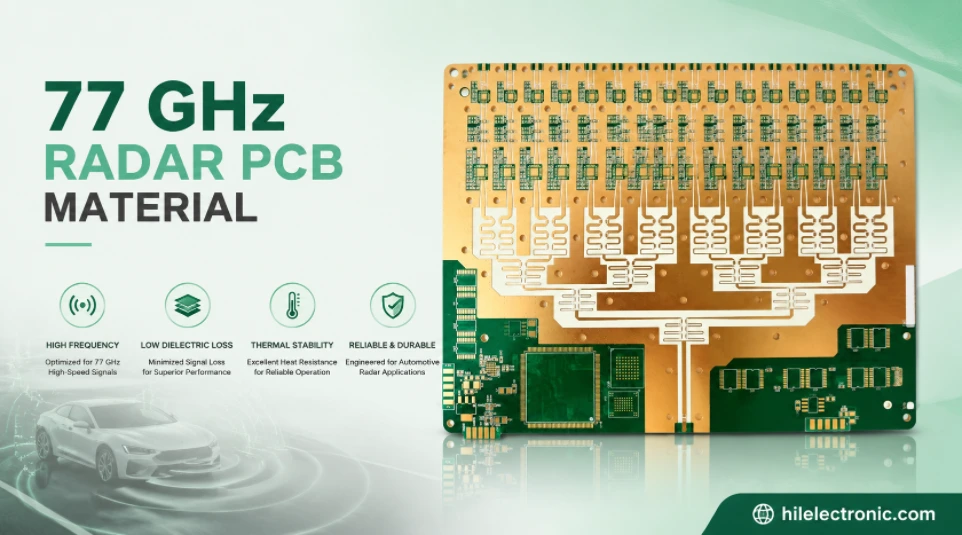
77 GHz Radar PCB Material Selection and Manufacturing Guide
Table of contentsWhat 77 GHz Changes in a PCBCommon 77 GHz...
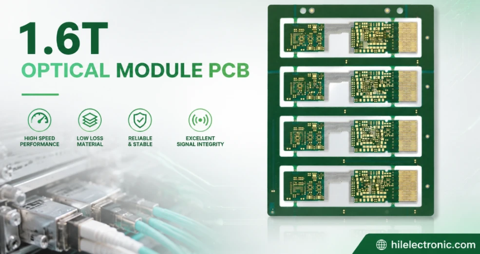
1.6T Optical Module PCB Manufacturing and Assembly Service
Table of contents1.6T Module Architectures and PCB...
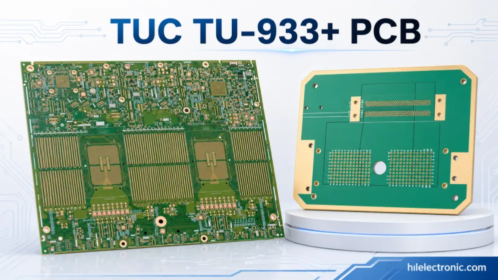
TUC TU-933+ PCB Manufacturing for Super-Low-Loss High-Speed Systems
Table of contentsWhat Is TU-933+ PCB Material?Why TU-933+...
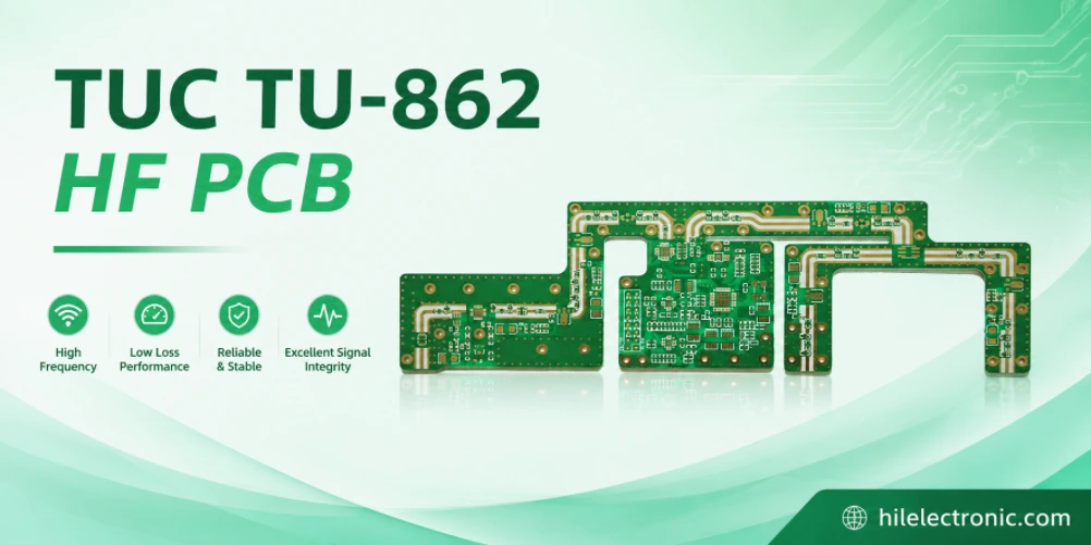
TUC TU-862 HF PCB Manufacturing and Assembly Service
Table of contentsWhat Is TU-862 HF?Why Choose TU-862 HF...
How to get a quote for PCBs
Let‘s run DFM/DFA analysis for you and get back to you with a report. You can upload your files securely through our website. We require the following information in order to give you a quote:
-
- Gerber, ODB++, or .pcb, spec.
- BOM list if you require assembly
- Quantity
- Turn time
In addition to PCB manufacturing, we offer a comprehensive range of electronic services, including PCB design, PCBA, and turnkey solutions. Whether you need help with prototyping, design verification, component sourcing, or mass production, we provide end-to-end support to ensure your project’s success.
For PCBA services, please provide your BOM (Bill of Materials) and any specific assembly instructions. We also offer DFM/DFA analysis to optimize your designs for manufacturability and assembly, ensuring a smooth production process.