
Back to blog
Exploring the Fundamentals of RF Circuits

RF Circuit PCB
RF PCBs, or radio frequency printed circuit boards, are essential components in modern electronic devices, enabling wireless communication and signal processing. Designing high-performance RF PCBs requires a comprehensive understanding of RF circuits and careful material selection. This article explores the fundamentals of RF circuits, the importance of RF PCB material selection, and the challenges and solutions in RF PCB design.
RF Circuit Basics
RF circuits are specialized circuits designed to operate at radio frequencies, enabling wireless communication and efficient signal processing. These circuits differ from lower frequency circuits in their design considerations, requiring meticulous attention to detail for optimal performance.
RF circuits are crucial components in devices such as smartphones, Wi-Fi routers, and satellite communication systems, enabling connectivity and signal processing. Understanding the basics of RF circuits is fundamental for designing high-performance RF PCBs that meet the demands of modern technology.
RF Circuit Design Considerations
Designing RF circuits involves careful consideration of factors such as frequency, impedance, and signal integrity. These factors are critical for ensuring optimal performance in RF PCBs.
One of the primary challenges in RF PCB design is impedance matching, aligning the impedance of various circuit elements for maximum power transfer and minimal signal reflections. Achieving proper impedance matching is crucial in high-frequency applications to prevent signal degradation.
Signal integrity is another critical consideration in RF PCB design, requiring precise engineering techniques to maintain signal quality at high frequencies. Factors such as trace length, routing, and electromagnetic interference must be carefully controlled to avoid signal distortion or loss.
RF Traces on PCB
RF traces are a critical component of RF PCB design, as they carry high-frequency signals that are sensitive to interference and signal loss. Optimizing RF trace design is essential for ensuring the reliable transmission of RF signals within electronic devices.
Key Considerations for RF Trace Design:
Trace Width: The width of RF traces is crucial for maintaining signal integrity. Wider traces reduce resistance and inductance, minimizing signal loss. However, wider traces can also increase the risk of signal crosstalk and interference, so a balance must be struck based on the specific requirements of the RF circuit.
Spacing Between Traces: The spacing between RF traces is important for minimizing crosstalk and interference. Closer spacing can improve signal integrity but may increase the risk of interference. Proper spacing is determined by the frequency of the RF signal and the requirements of the circuit.
Impedance Matching: Impedance matching is critical for ensuring maximum power transfer between components and minimizing signal reflections. Proper impedance matching is achieved by carefully designing the dimensions of RF traces and matching components such as capacitors and inductors.
Grounding: Proper grounding is essential for minimizing noise and interference in RF circuits. RF traces should be surrounded by a solid ground plane to provide a low-impedance return path for the RF signal.
Signal Routing: Careful routing of RF traces is necessary to minimize signal loss and interference. Traces should be kept as short and direct as possible, avoiding sharp bends and crossing other traces at right angles.
Shielding: In high-noise environments, shielding can be used to protect RF traces from external interference. Shielding can be achieved using grounded metal layers or conductive shielding materials.
Testing and Validation: Once the RF PCB is designed, it is essential to test and validate the performance of the RF traces using RF test equipment. This ensures that the PCB meets the required specifications for signal integrity and performance.
By carefully considering these factors and employing best practices in RF trace design, engineers can optimize the performance and reliability of RF PCBs for a wide range of applications.

PCB Material Selection
Selecting the right PCB material is crucial for optimizing the performance and functionality of RF PCBs. The choice of material directly impacts the electrical properties, thermal characteristics, and signal transmission capabilities of the PCB.
Ideal PCB materials for RF applications possess characteristics such as low dielectric loss, high thermal conductivity, and excellent signal transmission properties. These properties ensure minimal energy dissipation, effective heat dissipation, and reliable signal transmission within the RF circuitry.
Innovative RF PCB Applications
RF PCBs (radio frequency printed circuit boards) are at the forefront of innovative applications, enabling cutting-edge technologies across various industries. Here are some of the most innovative applications of RF PCBs:
- 5G Technology Integration: RF PCBs play a critical role in 5G technology, facilitating high-speed data transmission and enabling the massive connectivity required for 5G networks. These PCBs are designed to handle the high frequencies and complex signal processing demands of 5G communication, making them essential for the deployment of 5G infrastructure.
- IoT (Internet of Things) Connectivity: RF PCBs are key components in IoT devices, enabling wireless connectivity and data exchange between devices. These PCBs are used in smart home devices, industrial sensors, and wearable gadgets, among others, to enable seamless communication and integration within IoT ecosystems.
- Wearable Technology: RF PCBs are crucial for the development of wearable technology, powering devices such as smartwatches, fitness trackers, and health monitors. These PCBs enable wireless connectivity, sensor data processing, and energy efficiency, allowing for the creation of compact and functional wearable devices.
- Automotive Radar Systems: RF PCBs are integral to automotive radar systems, which are used for collision avoidance, adaptive cruise control, and other advanced driver assistance features. These PCBs enable the transmission and reception of radar signals, helping vehicles detect obstacles and navigate safely.
- Aerospace and Defense: RF PCBs are widely used in aerospace and defense applications for communication, radar systems, and electronic warfare. These PCBs are designed to meet stringent requirements for reliability, performance, and durability in harsh environments.
- Medical Devices: RF PCBs play a crucial role in medical devices, enabling wireless communication, data processing, and monitoring capabilities. These PCBs are used in devices such as MRI machines, patient monitoring systems, and implantable medical devices, where reliable performance is essential.
- Satellite Communication: RF PCBs are used in satellite communication systems to transmit and receive signals between satellites and ground stations. These PCBs enable high-speed data transmission over long distances, supporting critical communication infrastructure.
- Environmental Monitoring: RF PCBs are utilized in environmental monitoring systems to collect and transmit data on air quality, water quality, and other environmental parameters. These PCBs enable real-time monitoring and analysis of environmental conditions, supporting efforts to mitigate environmental impact.
Overall, RF PCBs are driving innovation across a wide range of industries, enabling the development of advanced technologies that enhance connectivity, efficiency, and functionality. As technology continues to evolve, the role of RF PCBs in enabling innovative applications is expected to expand, shaping the future of wireless communication and connectivity.
Future RF PCB Technology
The future of RF Circuits holds promising developments in enhancing performance, miniaturization, and integration with emerging technologies.
Advancements in RF PCB technology are aimed at achieving improvements in performance and efficiency. This involves optimizing signal transmission and reducing interference in high-frequency applications.
Miniaturization is another focus of future RF PCB technology, enabling the development of compact electronic devices without compromising performance. Miniaturized RF PCBs play a crucial role in portable devices, IoT sensors, and wearable technology.
Integration with emerging technologies such as 5G networks and IoT is also a key area of development. RF PCBs are being engineered to seamlessly integrate with these platforms, enabling innovative applications that leverage the capabilities of 5G technology and smart interconnected devices.
Conclusion
RF PCBs are essential components in modern electronic devices, enabling wireless communication and signal processing. Designing high-performance RF PCBs requires a comprehensive understanding of RF circuits and careful material selection.
By understanding the basics of RF circuits, the importance of PCB material selection, and the challenges and solutions in RF PCB design, engineers can develop high-performance RF PCBs that meet the demands of modern technology. With advancements in RF PCB technology and innovative applications on the horizon, the future of RF PCBs is promising, offering exciting possibilities for enhancing wireless communication and connectivity.
PCB & PCBA Quick Quote
Recommended Posts

PCB Current Calculator: Sizing Trace Width and Vias with the IPC-2221 Formula
Figure 1. Pcb Current Calculator reference image for PCB...

Microphone PCB Design: How the Board Itself Shapes Your Audio Quality
Figure 1. Microphone Pcb reference image for PCB...
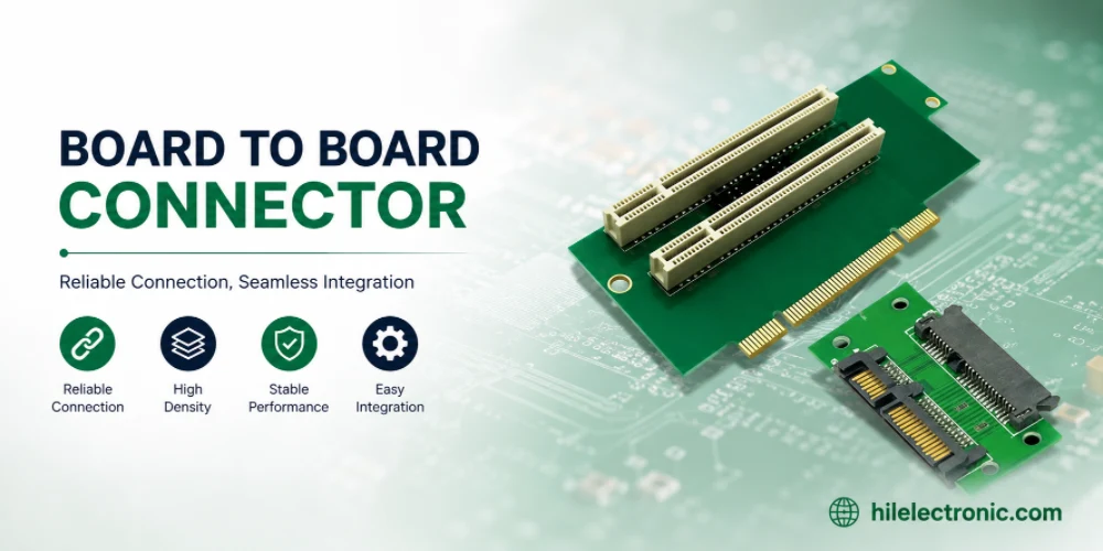
Board-to-Board Connector: Types, Specifications, and How to Select One
Figure 1. Board To Board Connector reference image for PCB...
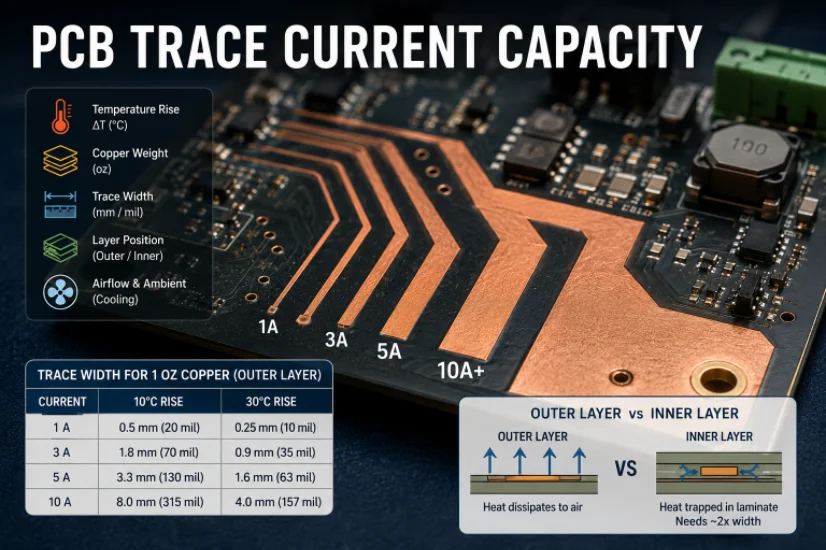
PCB Trace Width Calculator: How to Size Traces for Current, Voltage Drop, and Impedance
Figure 1. A PCB trace width calculator is a starting point...