
112G PCB Material Selection and High-Speed PCB Manufacturing
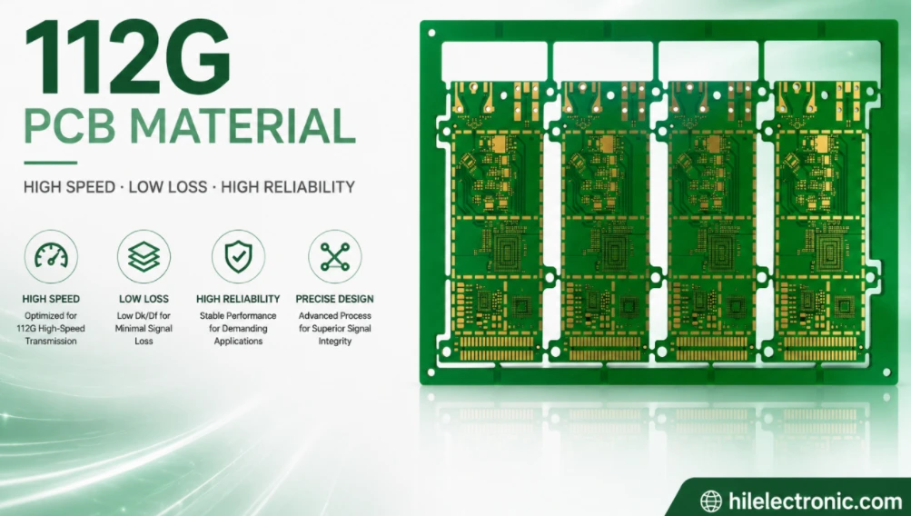
“112G PCB material” usually refers to laminate systems suitable for 112 Gb/s-per-lane electrical channels used in chip-to-module, chip-to-chip and backplane links. OIF CEI-112G defines several reach classes, so there is no single material that is correct for every 112G board.
Highleap Electronics manufactures the PCB and PCBA; we do not manufacture laminate. We help customers evaluate approved material options, then control stackup, copper, vias, connectors, assembly and testing.
What material is required for a 112G PCB? Select by channel reach and loss budget, not by data rate alone. Short VSR channels may use a different loss class from long backplane channels. Df, copper roughness, glass weave, dielectric thickness, via stubs and connector launches must be evaluated together.
What “112G PCB Material” Actually Means
A laminate datasheet gives bulk properties; a 112G channel is a manufactured interconnect. The finished channel includes trace geometry, copper profile, vias, pads, connectors, reference transitions and package breakouts.
VSR / chip-to-module
Short reach, but dense packages and connector launches make discontinuities critical.
MR / chip-to-chip
Longer routing raises loss and crosstalk sensitivity.
LR / backplane
Long channels and multiple connectors often require ultra-low-loss architectures or cable assistance.
Optical-module PCB
Short traces coexist with extreme density, power and mechanical constraints.
This is not a stand-alone material or interface decision. The final behavior is produced by the interaction of via stubs and connector discontinuities with dielectric loss, while copper roughness and glass-weave skew determine whether the same design can be repeated across panels and material lots. That is why Highleap begins with the board files instead of a generic product questionnaire.
A purchaser does not need to master every technical term in this section. What matters is that the files show the intended circuit and that the factory can identify the sensitive production variables. Highleap coordinates the review with the relevant specialists and explains the consequences in terms of feasibility, cost, lead time and acceptance.
Material Properties That Matter at 112G
| Property | Why it matters | Common mistake |
|---|---|---|
| Dissipation factor | Contributes to dielectric attenuation | Comparing values measured by different methods |
| Effective Dk | Controls impedance and delay | Using a generic datasheet number for every construction |
| Copper roughness | Increases conductor loss and can affect delay | Modeling smooth copper while ordering standard foil |
| Glass weave | Can create skew and local impedance variation | Ignoring glass style and routing orientation |
| Resin content | Changes Dk, pressed thickness and fill | Assuming all prepreg with the same glass style is equivalent |
| Thermal reliability | Supports high-layer-count lamination and assembly | Choosing only by low Df |
Generic datasheet values are not enough when ordinary electrical testing cannot detect a channel that passes schematic review but fails insertion-loss limits or unexpected skew between differential pairs. The review must use the exact core or prepreg, copper profile, finished thickness and via route. This is where one-to-one engineering support prevents the buyer from having to interpret multiple supplier documents alone.
Published Dk and Df values are only comparable when the test method, frequency, resin content and copper construction are understood. A lower nominal Df does not guarantee a lower-loss finished channel if the selected foil is rougher, the dielectric is thicker than modeled or the via field introduces large discontinuities. Highleap uses the exact available construction and finished copper assumptions when reviewing whether the requested material class is appropriate.
Common Material Classes for 112G PCBs
Depending on reach, designers may evaluate low-loss, very-low-loss, super-low-loss or ultra-low-loss thermoset systems. Examples include high-speed families from Panasonic, TUC, Isola, ITEQ, Nelco and other suppliers. Highleap does not treat these brands as automatic equivalents.
The production construction must define laminate and prepreg, glass style, resin content, copper foil and thickness. A family name such as “Megtron,” “ThunderClad” or “low-loss FR-4” is incomplete.
Repeatability is the main manufacturing test. A prototype can work even when the process window is broad, but volume production exposes variation in material lots, copper distribution, panel loading and plating. We place representative impedance and loss coupons, approved laminate and foil traceability, stackup and field-solver correlation and back-drill or HDI review in the production release to provide a stable comparison between lots. If EM-892K is on the approved-material shortlist, EM-892K fabrication for high-speed channels should be reviewed against the actual stackup and channel-loss requirements.
Design intent and factory compensation have different owners. The customer defines electrical and reliability requirements; Highleap applies the approved CAM, drilling, plating and lamination adjustments needed to reach the finished values. Any change that affects architecture or qualification is raised for approval instead of being hidden inside CAM processing.
Implications of Selecting Material by Df Alone
- Rough copper can create more loss than the dielectric improvement saves.
- Long via stubs can create resonances that dominate the channel.
- Glass-weave skew can reduce eye margin even when insertion loss is acceptable.
- Uncontrolled pressed thickness can move impedance and coupling.
- Connector launch errors can cause return-loss failures.
- A very low-loss material may add cost without measurable benefit on short channels.
Repeat production creates another risk: a later lot can use a different available construction while the nominal material family remains unchanged. Highleap records the approved stackup, copper, process assumptions and inspection method so prototypes and production are compared against the same release basis.
These risks should lower the effort required to contact the factory, not raise it. Once Highleap receives the Gerber or design files, we check approved laminate and foil traceability, stackup and field-solver correlation, back-drill or HDI review and representative impedance and loss coupons. Only decisions that materially affect function, compliance, price or delivery are returned to the customer.
112G Stackup and Via Strategy
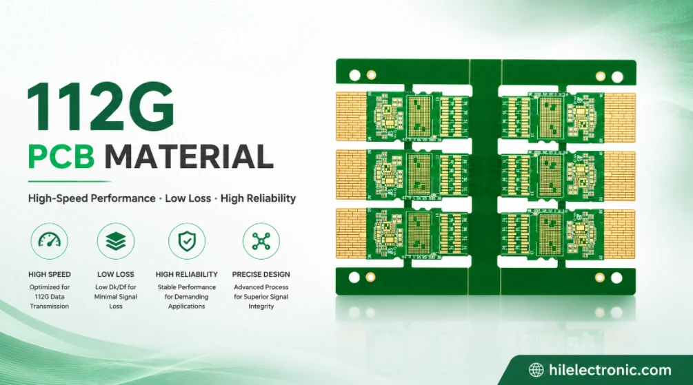
Highleap reviews signal-layer placement, reference continuity, copper profile, dielectric thickness, differential geometry and via transitions. Back drilling, blind vias or via-in-pad can reduce stubs, but each option has manufacturing and cost implications.
Back drilling
Requires a released drill table, target layer, residual-stub limit and inspection method.
HDI
Can shorten escape paths and remove through-via stubs, but sequential lamination and filled microvias increase complexity.
Coupons
Impedance, insertion-loss or S-parameter coupons should represent the actual production stackup and copper.
Repeatability is the main manufacturing test. A prototype can work even when the process window is broad, but volume production exposes variation in material lots, copper distribution, panel loading and plating. We place approved laminate and foil traceability, stackup and field-solver correlation, back-drill or HDI review and representative impedance and loss coupons in the production release to provide a stable comparison between lots.
The vertical path deserves the same attention as the routed trace. Every BGA breakout, reference-plane change, through-hole stub and back-drill residual length affects return loss and mode conversion. The stackup review therefore identifies the critical layer pairs, reference transitions and via geometry before panelization. Where HDI or back drilling is proposed, the manufacturing tolerance and inspection method are included in the release rather than left as an informal design assumption.
Highleap 112G PCB Manufacturing and Assembly
Highleap supports high-layer-count low-loss PCBs, HDI, sequential lamination, via-in-pad, back drilling, controlled impedance, fine lines, low-profile copper constructions, AOI, electrical test and cross-section. Optional TDR, S-parameter and insertion-loss testing can be included when the method and limits are defined.
For assembly, we provide component sourcing, SPI, BGA/LGA placement, AOI, X-ray, press-fit, through-hole and functional test.
Inspection is selected by package and defect risk. SPI controls paste deposition, AOI checks visible placement and solder features, and X-ray is used where joints are hidden. Special optical, RF or mechanical interfaces may also require fixtures, datum checks or customer handling instructions.
The assembly process begins with the bare-board construction. Warpage, copper balance, pad finish, via condition and thermal mass influence printing, placement and reflow. Highleap reviews the PCB and component layout together so a board that meets bare-board tests does not become a low-yield PCBA after high-value parts are loaded.
Production Release Requirements for 112G Channels
- Freeze the material system and allowed alternatives.
- Release the stackup with nominal and tolerance values.
- Identify copper foil and finished copper assumptions.
- Provide impedance and channel-loss requirements.
- Define back-drill or microvia structures.
- Provide connector and package models where launch tuning is required.
- Agree coupon design and test correlation before fabrication.
- Control assembly warpage, reflow and connector insertion.
Test coverage affects cost and schedule, so it should be proportional to risk. Critical structures receive direct verification; stable, noncritical features can rely on standard process control. The assigned engineer helps separate mandatory acceptance tests from useful engineering data and optional characterization.
Standard electrical test verifies opens and shorts, but it does not prove every performance requirement. Depending on the design, the plan may also use impedance coupons, back-drill inspection, microsection and optional insertion-loss or S-parameter verification. Highleap distinguishes production verification from full product qualification so the quoted test scope matches the decision the result is expected to support.
Send Your 112G PCB Design Files—We Will Clarify the Rest
For the first review, send the Gerber files or native PCB design files. A separate document listing every material, copper, loss and via requirement is not necessary when those notes already exist in the design data.
High-speed decisions are handled with an engineer
A dedicated Highleap engineer will review the channel structure with our signal-integrity and manufacturing team. We will confirm the appropriate material class, stackup, impedance, copper profile, HDI or back-drill needs through direct communication. Purchasing does not need to translate the design into a technical checklist before asking for a quotation.
This approach gives the customer a usable next action instead of a long checklist. Upload the board data first; Highleap will review manufacturability, identify the small number of decisions that need confirmation, and guide the project from quotation through prototype and repeat production.
112G PCB Cost and Material Optimization
The material price is only one part of total cost. Layer count, panel size, low-profile copper, sequential lamination, back drilling, coupons, test time and yield can be larger drivers. Highleap can compare constructions after the channel and qualification constraints are known.
Two boards with the same size and layer count can therefore have different prices. The relevant comparison is not unit material cost alone, but the manufacturing route, inspection burden, expected yield and amount of engineering or qualification work required for release.
Lead time is often controlled by material availability, special copper, supplier minimums, sequential processing or outside characterization. The engineer identifies the actual schedule constraint and checks whether an approved alternative can remove it without changing the product requirement.
Select the Whole Channel, Then Manufacture It Consistently
A “112G material” is not a guaranteed solution. Highleap connects the approved laminate to copper, stackup, via architecture, manufacturing, assembly and test so the built channel reflects the design assumptions.
Company roles also remain clear. Material suppliers manufacture laminate, prepreg or copper, and component suppliers manufacture devices and connectors. Highleap purchases approved inputs and converts them into finished PCBs and PCBAs with controlled processing, inspection and project communication.
The finished board must be released as one electrical, mechanical and manufacturing system. Highleap connects the customer files with representative impedance and loss coupons, approved laminate and foil traceability, stackup and field-solver correlation and the agreed inspection method. That documentation allows a successful prototype to be repeated when volume increases or the order returns later.
A material upgrade cannot compensate for a connector launch, long residual via stub or weak return path that already consumes the channel margin. Conversely, a short, well-controlled channel may not need the most expensive laminate available. Highleap’s role is to preserve the approved channel assumptions in fabrication and assembly, while making clear which limitations belong to the system design and which can be controlled by the PCB process.
Frequently Asked Questions
Does every 112G PCB need ultra-low-loss laminate?
No. Required loss class depends on reach, topology, copper, connectors, vias and system equalization.
Does Highleap manufacture the laminate?
No. We manufacture the PCB and PCBA using customer-approved laminate systems.
Can standard FR-4 support 112G?
Some very short structures may be possible, but it cannot be assumed. The complete channel must be modeled and validated.
Which is more important, Df or copper roughness?
Both matter. Their relative contribution depends on frequency, geometry, copper and channel length.
Can Highleap perform back drilling and HDI?
Yes, subject to project-specific DFM and the released via requirements.
What should purchasing send first for a 112G PCB quote?
Send the Gerber files or native PCB design files. A Highleap engineer will review the project one to one and coordinate the material, stackup, impedance and via questions with our engineering team.
Technical reference note: Material properties and interface descriptions must be checked against the current manufacturer datasheet, customer specification and applicable interface standard for the exact production construction. Highleap Electronics is the PCB fabrication and PCB assembly provider; laminate and component trademarks belong to their respective manufacturers.

Recommended Posts

Taconic RF 35 vs RO4350B PCB
Table of contentsRF-35 vs RO4350B Procurement and...

TMM4 Filter PCB Manufacturing
TMM4 filter PCB manufacturing is controlled by the...

TMM3 PCB Manufacturing for RF Modules
TMM3 PCB manufacturing is most useful where the RF module...

TMM6 PCB Fabrication
TMM6 fabrication is the process-control page for a mid-Dk...
How to get a quote for PCBs
Let’s run DFM/DFA analysis for you and get back to you with a report. You can upload your files securely through our website. We require the following information in order to give you a quote:
-
- Gerber, ODB++, or .pcb, spec.
- BOM list if you require assembly
- Quantity
- Turn time
For PCBA services, please provide your BOM (Bill of Materials) and any specific assembly instructions. We also offer DFM/DFA analysis to optimize your designs for manufacturability and assembly, ensuring a smooth production process.