
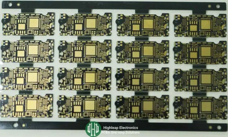
PCB Side Plating Solutions for High-Performance Electronics

PCB side plating, also referred to as edge plating, castellation, or side wall metallization, is a highly specialized feature in modern PCB manufacturing. This technique involves applying a conductive metal layer along the edges of a PCB to enhance electrical connectivity, structural rigidity, and electromagnetic compatibility (EMC). While widely adopted for its functional advantages, side plating requires a nuanced understanding of advanced manufacturing processes and precise implementation. Need reliable PCB side plating? Our advanced manufacturing ensures superior conductivity, grounding, and thermal management. Contact us to bring your high-frequency designs to life.
What is PCB Side Plating?
PCB side plating, or edge metallization, is an advanced process that involves applying a conductive metal layer along the vertical edges of a PCB). While it appears as a straightforward metallization, this technique addresses complex engineering challenges by enhancing electrical, mechanical, and electromagnetic characteristics. By turning the PCB’s edge into an active interface, side plating serves as a multi-functional element in high-performance circuit designs.
The core of side plating lies in its ability to extend the functionality of traditional PCB design boundaries. It enables the edge of the PCB to function as a reliable electrical conductor, a mechanical stabilizer, and an EMC (Electromagnetic Compatibility) shield, depending on the specific design requirements.
Why Choose PCB Edge Plating?
PCB edge plating is a versatile feature that significantly enhances both the mechanical and electrical properties of a PCB. Mechanically, edge plating strengthens the board’s periphery, providing added durability and resistance to wear during manufacturing, handling, or assembly. This extra reinforcement helps prevent edge cracking, delamination, or damage, especially in applications where the PCB is subjected to physical stress or vibration.
From an electrical perspective, edge plating serves as a crucial element for improving conductivity and electromagnetic shielding. By creating a continuous conductive path along the board’s edges, it enhances grounding and minimizes electromagnetic interference (EMI). This feature is particularly critical in high-frequency circuits where maintaining signal integrity is essential to overall performance.
Another key benefit of edge plating is its ability to aid in thermal management. The conductive edge helps dissipate heat more efficiently, distributing it away from high-power components and reducing the risk of localized overheating. This not only prolongs the lifespan of the PCB but also ensures stable performance under demanding operating conditions.
In summary, PCB edge plating is a valuable addition for designs that prioritize durability, signal integrity, and thermal efficiency. Its ability to improve both structural and functional reliability makes it indispensable for applications in high-frequency, high-power, or rugged environments.
Key Considerations for PCB Side Plating in Design
1. Defining Conductive Layers
In PCB designs incorporating side plating, it is essential to clearly define which internal layers connect to the plated edge. This ensures proper electrical functionality without unintended shorts or signal interference. High-frequency boards, where side plating is most common, demand precise alignment to maintain signal integrity and avoid parasitic effects. Designers should explicitly specify conductive layers in design files and use simulation tools to verify the electrical behavior of plated edges, particularly for RF and high-speed circuits.
2. Thorough Electrical Network Validation
High-frequency PCBs with side plating require rigorous validation of the electrical network. Misconnections or misalignments in the electrical paths can lead to significant performance degradation. Simulations should analyze factors like impedance matching, signal reflection, and crosstalk to ensure that the plated edges complement the overall design. This step is crucial for achieving high signal quality and reducing electromagnetic interference (EMI).
3. Consideration of Panelization and Reserved Connections
In SET panelized designs, additional considerations are needed to accommodate side plating. Reserved connection points must be allocated between individual boards on a panel to ensure consistent plating across shared edges. Proper spacing prevents inconsistencies and ensures smooth separation during routing. Design files should clearly define metallization boundaries and connection points to facilitate a seamless manufacturing process.
4. High-Frequency Design Considerations
For high-frequency boards, side plating must support controlled impedance and effective grounding. Proper alignment of the plated edge with return paths or ground planes helps reduce noise and ensures signal stability. In addition to functional performance, the plated edge acts as a critical EMI shield, protecting sensitive circuits from external interference and minimizing noise emissions. Simulation tools should be employed to confirm these properties before production.
5. Practical Tips for Reliable Side Plating
Maintaining appropriate copper clearances from the edges is essential to prevent shorts and ensure proper metallization. The continuity of plating across all designated edges must be verified to ensure consistent electrical and mechanical performance. Clear documentation of plating specifications, including layer connectivity and reserved areas, helps fabricators execute the design effectively. These steps are crucial for ensuring the reliability and functionality of PCBs with side plating, especially in high-frequency applications.

Key Responsibilities of CAM Engineers in PCB Side Plating
1. Gerber File Verification and Optimization
CAM engineers must carefully inspect Gerber files to ensure that side plating specifications are properly defined and manufacturable. This includes verifying the connectivity of side plating to the correct conductive layers, such as ground or signal planes, while maintaining clearances from unintended connections to avoid shorts. Missing or incomplete annotations, such as metallization thickness or edge plating areas, must be clarified with the design team and added to the files. Engineers also optimize edge copper boundaries to prevent issues like short circuits or interference during the plating process.
2. Panelization and Edge Connection Design
Proper panelization is critical for achieving consistent edge plating, particularly in SET configurations. CAM engineers must reserve sufficient connection tabs or bridges between PCBs on a panel to ensure continuous plating along shared edges. Adequate spacing is also required between boards to avoid damage to plated edges during CNC routing. Additionally, engineers optimize panel size based on manufacturing equipment, such as plating tanks and routers, to maximize process efficiency and minimize material waste.
3. ERP Workflow Integration and Process Notes
CAM engineers must incorporate specific side plating requirements into the ERP workflow to guide the manufacturing process. This involves adding steps for electroless and electroplating processes, defining plating thickness ranges (e.g., 25-50 µm), and specifying surface finishes like ENIG or HASL. Manufacturing notes must detail key operational instructions, such as “Use precise milling tools to prevent damage to plated edges” or “Reduce routing speeds to minimize burr formation.” These notes ensure that production teams understand and adhere to the special requirements of side plating.
4. Final Validation and Inspection
Before production begins, CAM engineers perform rigorous validations to ensure all files and processes meet quality standards. Electrical network validations confirm that edge plating connects to the correct layers without unintended shorts. Simulations of plating current distribution verify uniform thickness and adhesion. Once files are finalized, engineers generate production-ready layouts, including drill files and panelization instructions. Feedback loops with design engineers ensure that any issues are resolved, maintaining a high standard of manufacturability and performance in the finished product.
Types of PCB Edge Plating
1. Surround Edge Plating
Surround edge plating involves routing the PCB profile to expose the sidewalls after drilling. This routing process ensures that the sidewalls are accessible to the electroless copper base layer, allowing the edge plating to be applied simultaneously with the copper deposition in drilled holes. This method ensures seamless metallization along the PCB edges, making it suitable for applications requiring robust electrical connectivity.
2. Copper Clearance at Edges
To prevent damage to copper features during edge processing, maintaining a safe distance between copper traces and the PCB edge is essential. The standard minimum clearance distances are:
-
- 0.25 mm for outer layers with break routing.
- 0.40 mm for inner layers with break routing.
- 0.45 mm for all layers in designs with V-cut notches.
Adhering to these clearances ensures the structural integrity of the copper layers and reduces the risk of exposure during milling or routing.
3. Board Edge Plated-Through Holes (PTH)
Board edge PTH, also referred to as “butterfly holes,” are plated holes positioned at the edge of the PCB. These are designed for direct soldering or connecting two boards via connectors. To ensure manufacturing stability, there must be sufficient free space along the board’s edge to secure the PCB within the production panel. Pads on the top and bottom layers are mandatory to anchor the plating securely. For smaller plated holes, a gold finish is often preferred due to its enhanced solderability and durability.
4. Round-Edge Plating
Round-edge plating involves plating part or all of the PCB edge or internal cutouts, extending from the top to the bottom layer. This type of plating is often used to establish a strong ground connection or for shielding purposes, particularly in designs requiring robust EMI protection. The PCB profile is milled before the through-hole plating process to achieve the desired edge geometry. However, achieving 100% edge plating is challenging due to the need for routing tabs to secure the board during manufacturing. Electroless nickel immersion gold (ENIG) is the preferred surface finish for round-edge plating, offering excellent durability and conductivity.

Applications of PCB Edge Plating
-
-
Enhancing Conductivity
Edge plating improves the electrical conductivity along the PCB edges, ensuring seamless signal transfer and robust grounding in high-frequency circuits. -
Edge Connections
When external connections or inter-PCB links are required at the PCB edge, edge plating ensures reliable and durable contact points. -
Lateral Impact Protection
Plated edges provide additional mechanical strength, protecting the PCB from lateral impacts during handling or operation. -
Connecting Secondary Boards
Secondary PCBs can connect seamlessly to the main board via edge plating, eliminating the need for additional connectors or solder pads. -
Soldering for Better Fit
Plated edges create stronger solder joints, improving the fit and alignment of PCBs within assemblies, particularly in compact or modular designs.
-
PCB Side Plating: The Ultimate Solution for Modern Electronics
PCB side plating is not just a manufacturing step—it’s a strategic engineering solution that meets the rigorous demands of today’s advanced electronic designs. This innovative process combines state-of-the-art materials, precision manufacturing techniques, and thoughtful design principles to deliver unparalleled electrical performance, mechanical durability, and electromagnetic stability.
For industries working with RF technology, IoT modules, or high-speed digital circuits, side plating is indispensable. It enhances signal integrity, improves thermal management, and adds structural strength, making it an essential feature for engineers seeking reliability and top-tier performance.
Whether you’re designing for next-generation wireless communication or compact, high-frequency devices, side plating provides a proven pathway to success. Partner with us to unlock the full potential of your PCB designs. Let’s take your innovation to the next level—contact us today to explore tailored solutions and competitive pricing for PCB side plating!
Get a Free PCB & PCBA Quote

Recommended Posts

PCB Manufacturing Process Flow – Ultimate Guide Is Here
[pac_divi_table_of_contents...

Exploring PCB Surface Treatment: The Significance of ENIG and DIG
PCB Surface Treatment:ENIG PCB With the ever-evolving...

How PCB Dry Film Plays a Key Role in Enhancing PCB Reliability
PCB dry film pressing equipmentWhat is PCB Dry Film? Dry...
High-Quality Rigid PCB Circuit Board Fabrication Services
HDI Rigid PCBWhat are rigid PCB and flexible PCB? In the...
How to get a quote for PCBs
Let us run DFM/DFA analysis for you and get back to you with a report.
You can upload your files securely through our website.
We require the following information in order to give you a quote:
-
- Gerber, ODB++, or .pcb, spec.
- BOM list if you require assembly
- Quantity
- Turn time
In addition to PCB manufacturing, we offer a comprehensive range of electronic services, including PCB design, PCBA (Printed Circuit Board Assembly), and turnkey solutions. Whether you need help with prototyping, design verification, component sourcing, or mass production, we provide end-to-end support to ensure your project’s success. For PCBA services, please provide your BOM (Bill of Materials) and any specific assembly instructions. We also offer DFM/DFA analysis to optimize your designs for manufacturability and assembly, ensuring a smooth production process.