
Back to blog
PCB Plating Techniques: The Ultimate Guide for Success
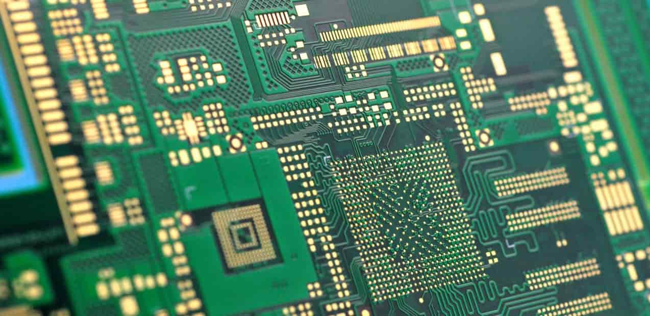
PCBs consist of a complex network of conductive traces and pads, typically made of copper, arranged on insulating substrates. To safeguard these vital components from corrosion, enhance electrical conductivity, and ensure their long-term reliability, the process of PCB plating is employed. This article delves into the intricacies of PCB plating, exploring its significance, materials used, the plating process, common methods, and the factors that influence successful plating.
The Significance of PCB Plating
PCB plating serves as a critical step in the PCB manufacturing process, offering several compelling benefits:
- Corrosion Protection: One of the primary functions of PCB plating is to shield the copper traces and pads from corrosion. Copper is susceptible to oxidation, which can degrade the electrical connections over time. Plating forms a protective barrier that ensures the PCB remains robust and reliable.
- Enhanced Electrical Conductivity: Plating contributes to improving the electrical conductivity of the PCB. This is crucial for the efficient flow of electrical signals across the board, reducing signal loss and ensuring the device’s proper operation.
- Solderability: PCB plating provides a conducive surface for soldering electronic components onto the board. Proper soldering is imperative for establishing dependable electrical connections, a cornerstone of PCB functionality.
- Durability: Plating renders the PCB more durable, safeguarding it from physical damage that may occur during manufacturing, assembly, or everyday usage. This durability extends the lifespan of the PCB and permits its utilization in demanding environments.
Materials Used in PCB Plating
The choice of plating material depends on specific application requirements. Common materials used for PCB plating include:
- Gold: Gold plating is prevalent due to its exceptional electrical conductivity, corrosion resistance, and durability. Its relatively soft nature also facilitates ease of processing during manufacturing.
- Silver: Silver, renowned for its high electrical conductivity, is favored for high-frequency applications. However, it is more prone to oxidation over time compared to gold.
- Nickel: Nickel is often employed as an underplating material due to its excellent adhesion properties. It offers a suitable base for subsequent plating layers, such as gold or silver.
- Copper: Copper is also used as an underplating material, providing an ideal surface for the adhesion of additional plating layers. It is an excellent conductor of electricity.
The PCB Plating Process
The PCB plating process involves several meticulous steps:
- Cleaning: The initial step is a thorough cleaning of the PCB to eliminate any contaminants, dirt, or oils present on the surface. Specialized chemical cleaning solutions are used for this purpose.
- Etching: Unwanted copper is removed from the PCB’s surface through a chemical etching process. This process selectively removes excess copper, leaving behind the desired copper traces and pads.
- Pre-Dip: After etching, the PCB is immersed in a pre-dip solution that prepares the surface for plating by promoting adhesion.
- Plating: Electroplating is the heart of the plating process. During this phase, a thin layer of metal is electroplated onto the copper surfaces. The PCB is submerged into an electrolytic solution, and an electric current is applied, causing metal ions in the solution to deposit onto the PCB’s copper, forming a protective metal layer.
- Post-Dip: Following plating, the PCB undergoes a post-dip process to ensure the plating layer is fully formed and adheres securely to the surface.
- Stripping (if necessary): In some situations, the plating layer may need to be removed, typically if issues with the plating arise. This is achieved through a chemical stripping solution that selectively removes the metal layer.
Common PCB Plating Methods for Manufacturing
The manufacturing of printed circuit boards (PCBs) involves various plating methods tailored to specific needs and requirements. Here, we delve deeper into these common PCB plating methods:
Selective Plating
Selective plating is a precision-focused technique that targets specific areas of the PCB for plating while leaving other regions untouched. This method is particularly useful when creating multi-layered circuits or when additional conductive pathways are needed in specific areas. By selectively applying plating to designated zones, manufacturers have greater flexibility and control over the PCB’s design and functionality.
Through-Hole Plating
Through-hole plating is a widely used method, especially in the production of multilayer PCBs. It involves the plating of metal through holes or vias that traverse the layers of the PCB. These plated-through holes serve as conduits, connecting different layers within the board. Through-hole plating is crucial for ensuring electrical continuity and signal transmission between different sections of the PCB. This method adds structural integrity and stability to the board, making it suitable for a wide range of applications.
Surface Mount Technology (SMT) Plating
Surface mount technology (SMT) plating is focused on the surface pads of the PCB. These surface pads are essential for attaching electronic components to the board. Plating the surface pads enhances their durability and electrical conductivity, ensuring reliable connections between the PCB and the components. SMT plating is especially relevant in modern electronics manufacturing, where miniaturization and densely populated PCBs are common. The robust surface finish provided by SMT plating is crucial for soldering components accurately, even in high-density layouts.
Each of these PCB plating methods serves a specific purpose and contributes to the overall functionality and reliability of the printed circuit board. Manufacturers carefully select the appropriate plating technique based on their design requirements and the intended application of the PCB.
Common Surface Finishes in PCB Plating
The choice of surface finish is a critical aspect of PCB plating, as it directly impacts the board’s performance and reliability. Here are several common surface finishes used in PCB plating, each with its unique properties and advantages:
Gold Plating
Gold plating is the most prevalent and widely favored surface finish in PCB manufacturing. Its popularity stems from its exceptional electrical conductivity, remarkable durability, and resistance to oxidation. Gold-plated PCBs are highly reliable, making them suitable for various applications, including those in harsh environmental conditions. The gold surface finish ensures stable and low-resistance electrical connections, making it a top choice for mission-critical electronic devices.
Electroless Nickel Immersion Gold (ENIG)
Electroless Nickel Immersion Gold (ENIG) is a surface finish process that involves depositing a thin layer of nickel onto the PCB’s surface, followed by a layer of gold. The nickel layer serves multiple purposes, including enhancing adhesion and providing a reliable base for the gold layer. ENIG offers excellent conductivity and corrosion resistance, making it a popular choice for applications where both electrical performance and reliability are paramount. It complies with industry standards and is especially suitable for fine-pitch components and complex PCB designs.
Tin Plating
Tin plating is an economically viable alternative to gold plating. While not as conductive as gold, tin provides good electrical conductivity and durability. It is commonly used as a surface finish in various applications. However, tin is more susceptible to oxidation compared to gold or ENIG, which can be a concern in certain environments. Proper handling and storage are necessary to maintain its performance over time.
Silver Plating
Silver plating is chosen for its exceptional electrical conductivity, which makes it ideal for high-frequency applications. Despite its impressive conductivity, silver is prone to oxidation, and its durability over time is comparatively lower than that of gold or ENIG. Silver-plated PCBs are often used in situations where the benefits of its high conductivity outweigh its potential longevity issues. To mitigate oxidation concerns, manufacturers may apply additional protective coatings or use silver in specialized applications where its advantages are crucial.
Selecting the appropriate surface finish for a PCB depends on the specific requirements of the application, cost considerations, and the desired balance between performance and longevity. Each surface finish has its strengths and limitations, and manufacturers carefully evaluate these factors to ensure that the finished PCB meets the intended design and operational criteria.
Factors Influencing Successful PCB Plating
The successful plating of a printed circuit board (PCB) is influenced by several critical factors, each of which plays a crucial role in determining the quality, reliability, and performance of the finished PCB. Here are the key factors that influence successful PCB plating:
Thickness of Plating:
The thickness of the plating layer is a fundamental factor that affects the PCB’s performance. The thickness determines the electrical conductivity, durability, and overall quality of the plating. A well-controlled and uniform plating thickness ensures consistent electrical connections and protection against corrosion. Manufacturers must adhere to precise plating thickness specifications to meet the requirements of the design and application.
Adhesion:
The adhesion of the plating layer to the PCB substrate is critical for ensuring a reliable and long-lasting finish. Proper adhesion prevents delamination or peeling of the plating over time, which can lead to electrical issues and reduced reliability. Factors influencing adhesion include surface preparation, cleaning processes, and the choice of plating materials. Adequate adhesion is essential for robust PCB performance.
Uniformity:
The uniformity of the plating layer across the entire PCB surface is essential for consistent electrical performance. Irregular plating thickness or variations in plating quality can result in uneven electrical connections and signal integrity issues. Manufacturers employ controlled plating processes to achieve uniformity and meet design specifications. Ensuring uniformity is especially critical in high-frequency or high-speed applications.
Surface Preparation:
Proper surface preparation is a crucial step in the PCB plating process. The PCB’s surface must be thoroughly cleaned and free from contaminants, oxidation, or residues before plating. Inadequate surface preparation can lead to poor adhesion and plating defects. Various cleaning methods and chemical treatments are employed to prepare the PCB surface for successful plating.
Choice of Plating Material:
The selection of the plating material has a significant impact on the PCB’s performance and functionality. Different materials, such as gold, silver, tin, or nickel, offer distinct properties and advantages. The choice of plating material depends on factors like electrical conductivity, durability, cost, and application-specific requirements. Manufacturers consider these factors to determine the most suitable plating material for a given PCB.
Plating Process Control:
Precision and control during the plating process are paramount. Manufacturers utilize advanced equipment and automated processes to ensure accurate plating results. Control parameters, including temperature, current density, plating time, and bath chemistry, must be carefully monitored and adjusted to meet the desired plating specifications. Process deviations can lead to plating defects and performance issues.
Design Considerations:
PCB design plays a significant role in plating success. Design factors such as the arrangement of traces, pads, and component footprints can affect plating quality and uniformity. Designers must follow industry guidelines and best practices to optimize the PCB layout for successful plating processes.
Quality Control and Inspection:
Rigorous quality control and inspection procedures are essential to verify the quality of the plated PCBs. Manufacturers conduct visual inspections, thickness measurements, adhesion tests, and electrical continuity checks to ensure that the plating meets the required standards. Quality control measures help identify and address any plating defects or issues promptly.
Environmental and Regulatory Compliance:
Compliance with environmental regulations and industry standards is crucial in PCB plating. Manufacturers must use environmentally friendly processes and materials while adhering to standards such as RoHS (Restriction of Hazardous Substances). Meeting these requirements ensures both the quality of the finished PCB and environmental responsibility.
Process Documentation and Traceability:
Thorough documentation and traceability throughout the plating process are essential for quality assurance and troubleshooting. Accurate records of process parameters, materials, and inspection results enable manufacturers to track and rectify any deviations or issues that may arise during plating.
Successful PCB plating is the result of meticulous attention to these influencing factors, ensuring that the final product meets the desired specifications, performs reliably, and withstands the rigors of its intended application. Manufacturers continually refine their plating processes and quality control measures to achieve consistent and high-quality PCBs.
Conclusion
In summary, PCB plating plays a pivotal role in the manufacturing of printed circuit boards, enhancing their durability, electrical conductivity, and corrosion resistance. This comprehensive process involves meticulous steps, careful material selection, and consideration of various plating methods and surface finishes. By understanding the significance of PCB plating and its associated intricacies, manufacturers can ensure that their PCBs meet rigorous performance and reliability standards. Ultimately, PCB plating stands as a cornerstone in the creation of electronic devices, safeguarding their functionality and longevity.
PCB & PCBA quick quote
Related Articles

Exploring PCB Surface Treatment: The Significance of ENIG and DIG
PCB Surface Treatment:ENIG PCB With the ever-evolving landscape of electronic design, the reliability and performance of PCBs hinge crucially on their surface finishes. Among the array of PCB Surface Treatment available, Immersion Gold stands out for its robust...

Enhancing PCB Reliability: Reduce PCB Dry Film Penetration
PCB dry film pressing equipmentWhat is PCB Dry Film? Dry film is a photosensitive material used in the production of PCBs to create the circuit pattern. It is applied to the surface of the copper-clad laminate and then exposed to UV light through a film mask...
High-Quality Rigid PCB Circuit Board Fabrication Services
HDI Rigid PCBWhat are rigid PCB and flexible PCB? In the realm of PCBs, two primary types exist: rigid PCBs and flexible PCBs, each with distinct characteristics and applications. Understanding the differences between these two types of PCBs can help determine the...
Take a Quick Quote