
Back to blog
8 Popular PCB Test Methods in PCB Manufacturing
The Critical Role of Testing in PCB Manufacturing and Assembly
PCBs are integral components across industries, from consumer electronics and appliances to aerospace systems and medical devices. They provide the foundation for mounting and interconnecting electronic components using conductive copper traces etched on an insulating substrate.PCB testing validates manufacturing processes to detect flaws in materials, fabrication, component placement, and soldering.
Considering the mission-critical nature of PCBs, comprehensive testing during design, fabrication and assembly is indispensable for ensuring reliable functionality under diverse operating conditions. This article provides a detailed overview of the key PCB testing techniques, parameters evaluated, defect detection capabilities and recommended best practices.Here’s a more in-depth look at the importance of testing in PCB manufacturing and assembly:
- Quality Assurance: PCBs are at the core of electronic systems, and any defects or issues in the PCB can lead to system failures or malfunctions. Testing helps identify and rectify such issues before the PCBs are integrated into final products, ensuring high-quality and reliable performance.
- Cost Reduction: Detecting and addressing defects early in the manufacturing process is much more cost-effective than discovering and fixing them after the products have been assembled. Testing helps reduce rework, scrap, and warranty claims, thereby saving both time and money.
- Reliability: PCBs are used in a wide range of applications, including critical systems like medical devices and aerospace equipment. Failure in such applications can have severe consequences, making reliability paramount. Testing helps ensure that PCBs meet the required reliability standards and can perform under extreme conditions.
- Defect Detection: PCB testing encompasses a variety of techniques to detect defects such as shorts, opens, soldering issues, component misplacement, and more. These defects can occur during manufacturing, and thorough testing is essential to identify and rectify them.
- Process Validation: PCB testing is not just about finding defects but also validating the entire manufacturing process. It ensures that the processes used for etching, drilling, soldering, and component placement are consistent and meet the required specifications.
- Functional Verification: Beyond physical defects, PCBs need to be functionally verified to ensure that they perform as intended. This involves testing the electrical connectivity, signal integrity, and functionality of the components on the PCB.
- Environmental Testing: Depending on the application, PCBs may be subjected to various environmental conditions, such as temperature extremes, humidity, and vibration. Environmental testing helps determine how well the PCBs can withstand these conditions without degradation in performance.
Fundamentals of PCB Testing
PCB testing refers to the validation processes applied during the manufacturing cycle to screen for flaws in materials, fabrication techniques, component placement and soldering integrity. Electrical continuity, impedance control and dielectric insulation are common parameters examined.
Thorough testing provides manifold benefits:
- Improves field reliability by detecting errors early
- Reduces manufacturing and warranty costs
- Accelerates product development through rapid design-test iterations
- Ensures regulatory compliance for mission-critical applications
The exponentially rising complexity of modern PCBs makes structured testing as per IPC standards critical for quality and reliability. Automated testing now delivers over 98% coverage through precision robotics and AI-powered image recognition.
Key PCB Defects and Failure Modes
The manufacturing of printed circuit boards (PCBs) involves a meticulous process, and any deviation can lead to defects that affect the functionality and reliability of the final product. Here’s a detailed look at common PCB defects and failure modes:
Common PCB Defects Detected During Manufacturing Testing:
- Dimensional Deviations: This includes boards shrinking or expanding beyond their specified tolerances, which can lead to misalignments of components and traces.
- Lamination Issues: Premature delamination can expose copper traces, leading to potential corrosion and failure of the electrical pathways.
- Etching Errors: Under-etching can leave unwanted copper on the board, causing weak traces, while over-etching can remove too much copper, leading to electrical shorts.
- Poor Soldering: Defects like cold solder joints, insufficient solder, and solder bridges can cause open circuits or short circuits, severely affecting the board’s functionality.
- Cracked Vias/Pads: Fractures in plated through-holes (vias) or pads can compromise the electrical continuity of the circuit.
- Contamination: Residues like flux or fingerprints can impact the performance of the PCB by causing leakage currents or other electrical issues.
Broader Product Failures Resulting from These Flaws:
- Electrical Shorts: Unintentional connections that create stray closed paths, leading to malfunction or damage to components.
- Open Circuits: Intended connections that remain unclosed, leading to signal loss and malfunctioning of the circuit.
- Signal Integrity Issues: Problems like reflections, delays, and noise that degrade the performance of high-speed circuits.
- Intermittent Faults: These are defects that are triggered only under specific conditions or stress, making them challenging to detect and diagnose.
- Cascading Failures: A single point of failure can trigger systemic crashes, affecting the entire board or even connected systems.
Importance of Testing Best Practices:
- Adopting comprehensive testing best practices is crucial in identifying and rectifying these defects early in the manufacturing process.
- This includes a range of tests like Automated Optical Inspection (AOI), In-Circuit Testing (ICT), Functional Testing, and others, each addressing different types of potential issues.
- Early detection through these tests not only ensures the reliability of the PCB but also saves costs associated with rework or failure in the field.
In conclusion, understanding and addressing these common PCB defects during the manufacturing process is essential for ensuring the quality and reliability of the final product. Regular and thorough testing is key to identifying potential issues early on, thus preventing cascading failures and maintaining the integrity of the PCB in its intended application.
Popular PCB Testing Methods
There are several testing methods available to assess the quality of a PCB. These methods include in-circuit testing, flying probe testing, automated optical inspection (AOI), and functional testing. However, it is important to consider certain factors before deciding which method to use.
For instance, burn-in testing is not suitable for every project, but it can be beneficial in preventing embarrassing product launches and potentially identifying issues that may shorten the product’s lifespan. However, it is important to note that burn-in testing can subject the PCB to additional stress, which may exceed its normal operating conditions. It is also worth mentioning that the effectiveness of burn-in testing can be influenced by the presence or absence of defects in the board.
Each testing method has its advantages and limitations, and the choice of method should be based on the specific requirements of the project and the desired level of quality assurance. By carefully considering these factors and selecting the appropriate testing method, manufacturers can improve the reliability and performance of their PCBs.The following are currently popular testing methods:
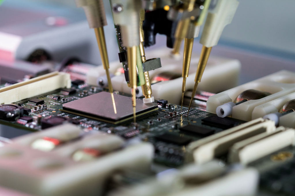
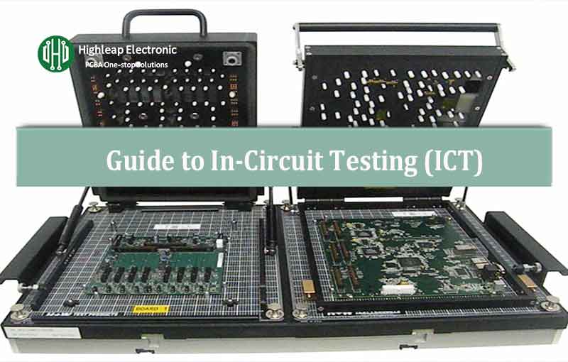
In-Circuit Testing
In-circuit testing (ICT) is an essential and highly reliable method for ensuring the quality and functionality of printed circuit boards (PCBs). Here’s a breakdown of its key aspects:
- Automated Testing of Individual Circuits: ICT involves automated testing of each circuit on a board. It checks for proper component values and ensures these are within specified tolerances, reducing the chances of human error.
- Fault Detection: The method is effective in detecting faults such as incorrect component orientation, short circuits, and other potential issues that could affect the functionality of the PCB.
- Common Test Types:
- Peel Test: Measures the strength required to peel a lamination from a PCB, indicating the quality of lamination.
- Solder Float Test: Assesses whether solder has adequately penetrated the metal surfaces, which is crucial for a robust solder joint.
- Solderability Test: Determines how well solder adheres to the PCB components.
- Surface Mount Simulation: Tests the PCB’s ability to withstand conditions experienced during surface mount assembly processes.
- Wetting Balance Analysis: Evaluates the wetting properties of solder on the PCB components.
- Burn-in Testing: This form of ICT involves using a high-voltage power supply to simulate operating conditions of the circuit board. While effective in detecting latent defects, burn-in testing carries a risk of damaging components and is typically used in conjunction with other testing methods.
- Importance in PCB Manufacturing: Testing PCBs is critical to avoid failures due to poor quality or design flaws. Since PCB failures can be costly, thorough testing is vital, regardless of whether the PCB is manufactured in-house or outsourced. This ensures that the final product delivered to customers is of high quality and reliability.
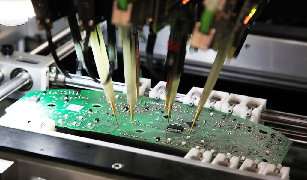
Flying Probe Testing
Flying probe testing is a method used in the quality control of printed circuit boards (PCBs), offering several advantages, especially for specific production scales and types. Here’s an overview of its key aspects:
- Cost-Effectiveness and Efficiency: One of the primary benefits of flying probe testing is its cost-effectiveness. It is highly efficient in detecting faults on PCBs, making it a practical choice for certain types of PCB production.
- Suitability for Prototypes and Low-Volume Production: Flying probe testing is particularly well-suited for prototypes and low-volume production runs. This is due to its flexible nature and the ease with which it can be set up for different PCB designs.
- Limitation for High-Volume Production: Despite its advantages, flying probe testing is not ideal for high-volume production. The nature of the testing method, which involves individual probes moving to test different parts of the PCB, makes it less efficient for large-scale production where speed is crucial.
- Methodology: In flying probe testing, power and electrical test signals are applied to specific probe locations on the PCB. The results of these measurements indicate whether there’s a fault in the circuit. A deviation from expected results suggests that the PCB does not meet the required standards.
- Accuracy and Coverage: This method is often considered more accurate than traditional in-circuit testing. It can test up to 99% of the PCB, providing a comprehensive assessment of the board’s functionality.
- Simultaneous Multiple Measurements: Multiple probes are used in flying probe testing, allowing for simultaneous measurements at different points on the PCB. This multipoint approach reduces the overall time needed for each test.
- Design Considerations: It’s important for the PCB design to include a “non-tented” specification to prevent the probes from touching the component legs, which could lead to inaccurate readings or damage.
- Comparative Advantage Over In-Circuit Testing: In terms of cost and the number of probes required, flying probe testing is less expensive than in-circuit testing. Its requirement for only a small number of test probes makes it more suitable for smaller-scale or less complex PCB production.
Automated Optical Inspection (AOI)
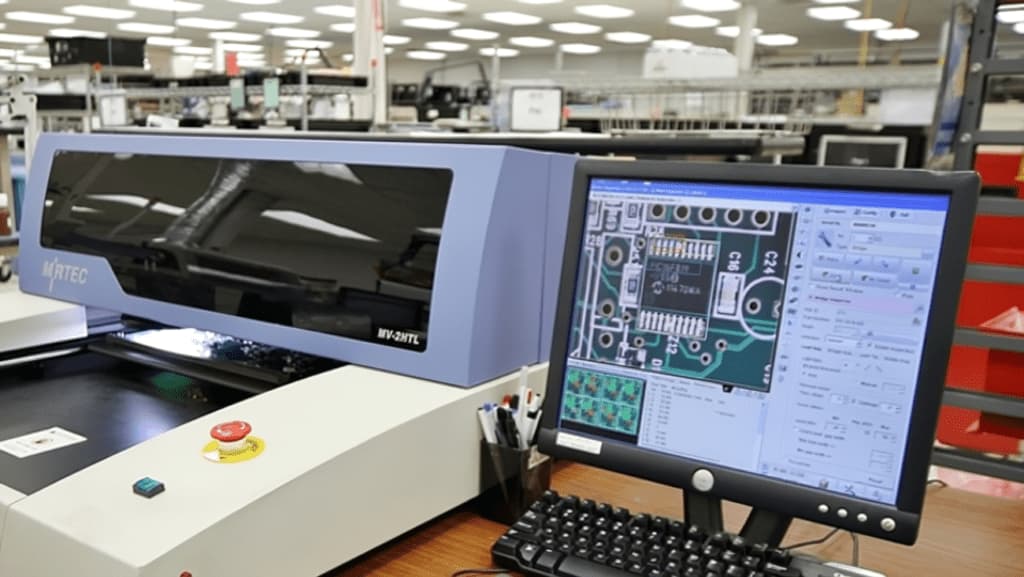
Automated Optical Inspection (AOI) is a crucial technology used in the manufacturing of printed circuit boards (PCBs) to ensure quality and accuracy. Here are the key aspects of AOI:
- Use of Cameras and Microscopes: AOI systems utilize multiple cameras and microscopes to capture detailed images of the PCBs. These images are then used for inspection purposes.
- Comparison with Schematics: The captured images are compared against the board’s schematic or a “golden board” (a reference board known to be defect-free) using specialized software. This comparison helps identify any discrepancies or defects.
- Early Detection of Problems: By closely inspecting each board, AOI allows for the early identification of a variety of problems, which is essential in preventing defective products from moving further down the production line.
- Detection Capabilities:
- Etching Issues: It can detect under and over-etching problems.
- Soldering Defects: Issues like solder gap and excess solder are identifiable.
- Component Defects: Missing components, incorrect component values, and improper placement or alignment are detectable.
- Lifted Lead Deficiencies: It can identify issues with lifted leads on components.
- BGA Shorts and Open Circuits: AOI can spot shorts and open connections in Ball Grid Array (BGA) packages.
- Non-Contact Inspection Method: As a non-contact visual inspection technique, AOI is adept at identifying both minor quality defects and more significant catastrophic failures without physically touching the PCB.
- Accuracy: AOI is renowned for its accuracy in detecting defects, making it one of the most reliable methods for PCB inspection.
- Flexibility in Manufacturing Process: AOI systems can be integrated at various stages of the PCB manufacturing process—before, during, or after reflow soldering, which is where most nonconformances tend to occur.
- Immediate Correction of Issues: The placement of AOI systems at strategic points in the production line allows for immediate correction of any issues detected. This proactive approach reduces the likelihood of rejecting products at the final inspection stage and improves overall manufacturing efficiency.
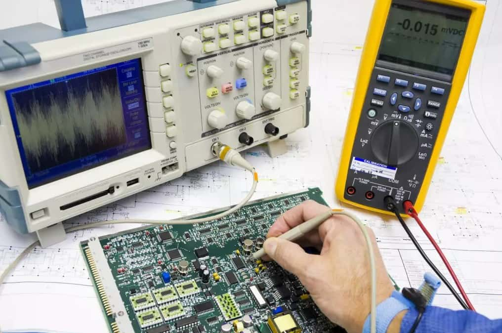
Functional Testing
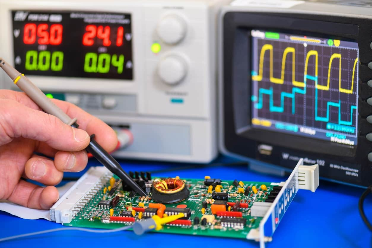
Functional testing in the context of PCB manufacturing is a critical step in ensuring that the final product operates as intended. Here’s an overview of how the process works and what it entails:
- Examination of Physical Components: Functional testing involves a thorough examination of the physical components of a PCB. This includes assessing the signals produced by the board and the interconnections between various components.
- Testing Fit and Function of Sub-Components: A significant aspect of functional testing is to verify the fit and function of sub-components. This ensures that all parts of the PCB are correctly aligned and interact as intended.
- Ensuring Intended Functionality: The primary purpose of functional testing is to confirm that the final product will function as designed. This includes checking all operational aspects of the PCB to ensure they meet the design specifications.
- Different Levels of Testing: Functional testing can range from basic tests, such as an on/off power test, to more complex procedures using specialized testing software. The level of testing depends on the complexity of the PCB and the requirements of the final product.
- Goal of Identifying and Correcting Problems: The ultimate goal of functional testing is to identify and rectify any issues that might arise after a product is completed. This proactive approach helps in preventing malfunctioning products from reaching customers.
- Simulation of Board Operation: To ensure proper operation, the process involves simulating the board’s functioning by testing its digital and analog signals. This simulation is crucial for detecting any functional anomalies or circuitry problems.
- Use of Specific Software for Detection: In many cases, specific software is employed during the testing process to aid in the detection of circuitry issues, enhancing the accuracy and efficiency of the test.
- Manual Inspections: Alongside automated testing, manual inspections might be conducted to assess different aspects of the PCB’s manufacturing process, ensuring that all quality standards are met.
In summary, functional testing in PCB manufacturing is a comprehensive process that evaluates the physical and operational aspects of a circuit board. It ranges from basic power checks to complex simulations and software-based testing, all aimed at ensuring that the PCB operates correctly and meets its design specifications before being shipped to the customer. This testing is crucial for maintaining high product quality and customer satisfaction.
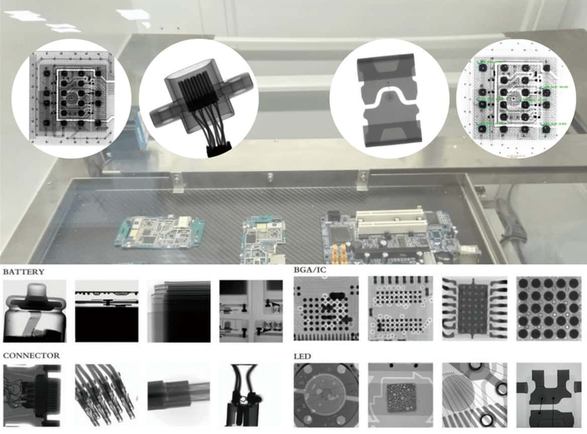
Automated X-ray Inspection (AXI)
Automated X-ray Inspection (AXI) is a sophisticated technique used in the testing of printed circuit boards (PCBs), leveraging X-ray technology to provide detailed insight into the board’s internal structures. Here’s a breakdown of AXI’s features, advantages, disadvantages, and applications:
Features of AXI
- Use of X-rays: AXI distinguishes itself from other inspection methods by using X-rays, which can penetrate the PCB and component bodies.
- Visualization of Solder Joints: It allows for the visualization of solder joints in both 2D and 3D, making it highly effective in inspecting areas that are not visible to the naked eye or through other optical methods.
- Ideal for Hidden Joints: AXI is particularly useful for inspecting ball grid arrays (BGA) and other underside pads where joints are hidden.
- Detection of Solder Voids: Unlike other optical inspection techniques, AXI can detect solder voids, which are critical defects that can affect the reliability of the PCB.
Advantages
- High Defect Detection Rates: AXI can achieve some of the highest defect detection rates among all PCB testing methods.
- Emphasis on Solder Joint Quality: The focus of AXI is on the quality of solder joints, rather than just the connections, providing a more comprehensive assessment of PCB integrity.
Disadvantages
- Time-Consuming and Cost-Intensive: The process can be slower and more expensive compared to other inspection methods.
- Need for Skilled Operators: Operating AXI equipment and interpreting the results require well-trained and experienced personnel.
Application
- High-Volume Production: AXI is well-suited for high-volume PCB production where its high defect detection rate can justify the time and cost involved.
- Boards with Chip Components: It is particularly valuable for boards that have chip components with hidden pads, as these are challenging to inspect using traditional methods.
In summary, Automated X-ray Inspection is a highly effective method for PCB testing, particularly in scenarios where internal or hidden defects need to be identified. Its ability to detect solder voids and focus on solder joint quality makes it a valuable tool in ensuring the reliability of PCBs, especially in high-volume production environments. However, the cost and time implications, as well as the need for skilled operators, are important factors to consider when integrating AXI into the manufacturing process.
Visual Inspection
Visual inspection is a fundamental method in the testing of printed circuit boards (PCBs), relying on the expertise and visual acuity of technicians to identify defects. Let’s break down its aspects:
Description of Visual Inspection
- Manual Testing Method: It is a part of manual testing, where skilled technicians visually check for defects.
- Scope of Inspection: The inspection typically covers aspects like weld quality, placement of components, and the application of the solder mask.
- Importance in PCB Inspection: Despite its simplicity, visual inspection is a crucial and basic method for ensuring the quality of PCBs.
Advantages
- Ease of Setup: It is straightforward to implement, requiring no complex machinery or software.
- Cost-Effectiveness: Visual inspection is one of the most affordable options in PCB testing.
- Detection of Major Solder Defects: It is particularly effective in spotting significant solder-related issues.
Disadvantages
- Time-Consuming and Labor-Intensive: It requires considerable manual effort and time.
- Inconsistency and Human Error: The effectiveness heavily relies on the skill and concentration of the technician, leading to potential inconsistencies and errors.
- Limited Scope: Only visible solder joints and defects can be inspected, leaving potential internal or microscopic issues undetected.
Application
- Suitability for Simple Designs: Visual inspection is most applicable to PCBs with simple designs and larger components, where defects are more likely to be visible to the naked eye.
In summary, while visual inspection is a basic and cost-effective method in PCB testing, its effectiveness is limited by its reliance on human skill and its inability to detect more subtle or internal defects. It is most suitable for simpler PCB designs with fewer and larger components. For more complex PCBs, integrating visual inspection with other advanced testing methods like Automated Optical Inspection (AOI) or In-Circuit Testing (ICT) can provide a more comprehensive quality assurance approach.
Burn-in Testing
Burn-in testing is an essential procedure in the electronic manufacturing process, particularly in ensuring the reliability and longevity of electronic devices such as printed circuit boards (PCBs). Here’s an overview of the process, its benefits, and its applications:
- Process Description: Burn-in testing involves subjecting electronic devices to prolonged periods of operation at maximum power levels. This process typically lasts between 48 to 168 hours.
- Stress Conditions: The components are exposed to high voltages, extreme temperatures, and other high-stress conditions during this test. This simulates long-term operation in a condensed time frame.
- Intensive Testing Nature: Often referred to as the “infant mortality process”, burn-in testing is designed to be highly intensive, pushing components to their operational limits.
Benefits of Burn-in Testing
- Elimination of Premature Failures: The primary benefit is the identification and elimination of components that fail prematurely. By weeding out these weak components early, the overall reliability of the product increases.
- Reduction of Field Failures: By ensuring that only robust and durable components make it past the testing phase, the likelihood of problems occurring in actual use (in the field) is significantly reduced.
- Identification of Vulnerable Components: Burn-in testing not only removes current failures but also helps in identifying components that are more susceptible to future failures under stress.
Application and Importance
- Quality Assurance: This testing is a critical part of quality assurance in the electronic manufacturing process, ensuring that products are durable and reliable.
- Reliability in Harsh Conditions: It is particularly important for devices that will be used in harsh environments or under intense operational conditions.
- Preventing Early Life Failures: By simulating extended use, burn-in testing helps in ensuring that products do not fail shortly after deployment, which is crucial for consumer trust and brand reputation.
In summary, burn-in testing is a rigorous and crucial step in the manufacturing of electronic devices. Its intensive nature helps in identifying and eliminating early-life failures, ensuring that the final products are reliable and capable of withstanding the stresses of actual use. This process is integral to delivering high-quality, durable electronics to consumers and industries alike.
Boundary Scan Test
Boundary Scan Testing, commonly known as JTAG (Joint Test Action Group) testing, is a widely used method for testing interconnections on printed circuit boards (PCBs), especially in complex or densely packed boards. Here’s an overview of its process, advantages, and applications:
Process of Boundary Scan Testing
- Testing Interconnections: The primary purpose of boundary scan testing is to test the interconnections between components on a PCB. This includes checking for open circuits, short circuits, and proper connectivity.
- Use of Test Access Ports (TAPs): The test involves inserting test data (batteries) into leads that connect the internal circuitry of the chips to their external pins. This data is then circulated through the circuitry to test its functionality.
- Non-Intrusive Testing: Unlike some other testing methods, boundary scan does not require physical access to every node on the PCB. This is particularly useful for multi-layered or high-density boards where physical access to all nodes is challenging.
Advantages
- Suitable for Complex PCBs: Boundary scan is ideal for modern, complex PCBs with multiple layers and high densities.
- Comprehensive Testing: It allows for thorough testing of a board’s interconnections without the need for physical probes or test points on every node.
- Flexibility: The method can be adapted for various applications beyond just testing interconnections.
Applications
- System-Level Testing: It can be used for overall system checks to ensure all components on a PCB are functioning correctly in the context of the entire system.
- Memory Testing: Boundary scan is effective in testing memory components on a PCB.
- Programming Flash Memory: It can be used to program flash memory chips on a PCB, which is a crucial step in many electronic devices.
- CPU Emulation: The technique allows for emulating the operation of a central processing unit (CPU), which can be crucial for diagnostics and testing.
- Detecting Manufacturing Defects: It is also widely used in the manufacturing process to identify defects and ensure quality control.
In summary, Boundary Scan Testing is a versatile and effective method for testing PCBs, particularly those that are dense or have complex layouts. Its ability to test without needing physical access to every node and its adaptability for various applications make it an invaluable tool in both the manufacturing and development phases of electronic devices.
PCB & PCBA quick quote
Related Articles
How to Test a Circuit Board?
[pac_divi_table_of_contents title="On this article" default_state="closed" included_headings="off|on|on|off|off|off" exclude_headings_by_class="on" active_link_highlight="on" level_markers_3="icons" title_container_padding="10px|15px|10px|15px|true|false"...
PCB Quality: The Definitive Guide to In-Circuit Testing (ICT)
[pac_divi_table_of_contents title="On this article" default_state="closed" included_headings="off|on|on|off|off|off" exclude_headings_by_class="on" active_link_highlight="on" level_markers_3="icons" title_container_padding="10px|15px|10px|15px|true|false"...
Understanding Crystal Oscillators and Their PCB Layout
[pac_divi_table_of_contents title="On this article" default_state="closed" included_headings="off|on|on|off|off|off" exclude_headings_by_class="on" active_link_highlight="on" level_markers_3="icons" title_container_padding="10px|15px|10px|15px|true|false"...
Take a Quick Quote