Back to blog
Comprehensive Overview of PLCC Packages in Electronic Device Manufacturing

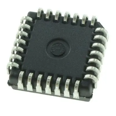
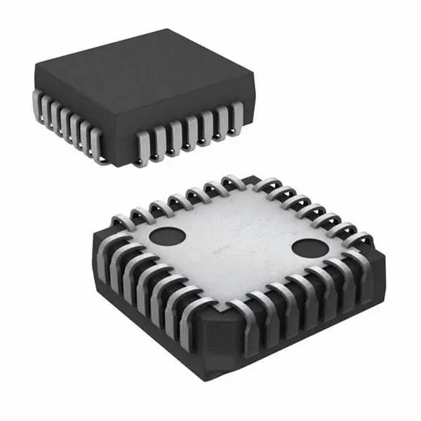
PLCC Package
Plastic Leaded Chip Carrier (PLCC) packages play a vital role in electronic device manufacturing. Despite the rise of newer IC packages like QFP and BGA, PLCCs remain relevant in specific applications, particularly in legacy systems. This article provides an exhaustive overview of PLCC packages, covering their design, types, advantages, applications, troubleshooting, and repair.
What is a PLCC Package?
PLCC packages are surface-mount integrated circuit (IC) packages with leads extending from all four sides, designed to be soldered onto a PCB. They offer a square or rectangular shape and can contain anywhere from 20 to over 84 pins. The top surface often includes a window for visual inspection of the IC.
The PLCC package was introduced as a more robust and reliable alternative to earlier IC packages. Over the years, it has seen widespread use in various applications, although newer packages like QFP and BGA have become more popular. However, PLCCs are still used in older electronic devices and specific modern applications where their unique characteristics are beneficial.
Design and Construction of PLCC Packages
Materials and Manufacturing Process
- Plastic Body: The body of a PLCC is typically made from a thermoset plastic, offering durability and a protective environment for the IC.
- Leadframe: Made from copper or a copper alloy, the leadframe supports the leads and connects to the IC chip.
- IC Chip Attachment: The IC chip is attached to the leadframe using wire bonding, where thin wires connect the chip pads to the leads.
- Mold Compound: An epoxy mold compound encapsulates the assembly, providing additional protection.
- Package Marking: Essential information such as manufacturer, part number, and date code is printed or laser-etched on the package.
Advantages of PLCC Packages
- Cost-Effective: Economical to produce, making them suitable for a wide range of applications.
- Versatility: Available in various sizes and pin counts, fitting diverse circuit requirements.
- Ease of Assembly: Designed for automated assembly, reducing manufacturing costs and time.
- Inspection-Friendly: The window on the top surface allows for easy visual inspection.
Disadvantages of PLCC Packages
- Thermal Performance: Limited compared to QFP and BGA packages, posing challenges in high-power applications.
- Reliability: Less reliable than ceramic packages in extreme environments.
- Signal Speed: Longer signal paths can limit performance in high-speed applications.
- Pin Density: Limited space for pins, restricting use in high-pin-count applications.

PLCC Package
Types and Sizes of PLCC Packages
PLCC packages come in several variants, each tailored to specific applications:
- Standard PLCC: Versatile, available with 20 to 84 pins.
- Miniature PLCC: Smaller body and pin count (16 to 52 pins) for compact applications.
- Thin PLCC: Thinner profile, suitable for space-constrained designs.
- Quad PLCC: Leads on only two sides, supporting higher pin counts (44 to 84 pins).
- Enhanced PLCC: Includes a heat sink for better thermal management in high-power applications.
- Ceramic PLCC: Offers superior thermal performance and reliability for extreme conditions.
Applications of PLCC Packages in PCB Design
PLCC packages are versatile and find use in various types of PCBs across different industries due to their robustness, ease of assembly, and compact size.
- Consumer Electronics PCBs: Used in devices like TVs, digital cameras, and gaming consoles where compact size and cost-effectiveness are critical.
- Automotive Electronics PCBs: Ideal for engine control units, sensors, and lighting systems, valued for their reliability and durability in harsh conditions.
- Medical Device PCBs: Employed in diagnostic instruments, patient monitoring systems, and other medical electronics where precision and reliability are paramount.
- Aerospace and Defense PCBs: Utilized in avionics, communication systems, and other critical applications that require high durability and performance in extreme environments.
- Industrial Equipment PCBs: Found in PLCs, motor drives, and power supplies, appreciated for their accuracy and dependability in industrial automation and control systems.
Specific PCB Types
- Single-Layer PCBs: Used for simple, low-density applications where PLCCs can be easily accommodated due to their straightforward layout.
- Multi-Layer PCBs: Essential for high-density and complex circuits found in advanced consumer electronics, automotive, aerospace, and medical devices. The multiple layers allow for intricate routing and increased functionality.
- Rigid-Flex PCBs: Ideal for applications requiring both flexible and rigid areas within the same board, such as in wearable technology and compact medical devices. PLCCs fit well due to their reliable lead attachment.
- High-Frequency PCBs: Used in communication devices and advanced electronics requiring stable performance at high frequencies. PLCCs provide consistent connectivity and signal integrity.
- High-Density Interconnect (HDI) PCBs: Suitable for miniaturized applications with high component density, such as smartphones and tablets. PLCCs’ compact design allows for efficient use of limited space.
By understanding the types of PCBs that commonly use PLCC packages, designers can better appreciate the versatility and applications of these components in modern electronics.

PLCC Packages
How to Reasonably Use PLCC Packaging
To reasonably use PLCC (Plastic Leaded Chip Carrier) packaging in your electronic designs, start by ensuring that the package fits the layout and design requirements of your PCB, including verifying the pin count and dimensions. Pay special attention to thermal management, as PLCCs have limited thermal performance; employ adequate cooling solutions like heatsinks or improved airflow to handle heat dissipation in high-power applications.
Utilize precise soldering techniques to avoid common issues such as cold joints or bridging, and leverage the inspection window on the PLCC package for visual checks. Additionally, use specialized testing equipment to verify IC functionality before and after soldering. Deploy PLCC packages in applications where their characteristics are most advantageous, such as consumer electronics, automotive systems, medical devices, aerospace, and industrial equipment.
For complex designs or repairs, consider enlisting professional services to ensure optimal implementation and troubleshooting. This leverages their advanced skills and specialized tools, ensuring the PLCC packages are used to their full potential, enhancing the performance and reliability of your electronic devices.
Troubleshooting and Repair of PLCC Packages
Troubleshooting PLCC packages can be complex due to their dense pin configuration. Here are detailed steps to diagnose and repair these packages:
- Visual Inspection: Begin by meticulously examining the package for any physical damage, such as cracks, discoloration, or bent pins. This initial step can help identify obvious defects that might be causing the issue.
- Testing the IC: Utilize specialized diagnostic equipment to probe individual pins and test the functionality of the integrated circuit. This helps pinpoint specific internal failures within the IC.
- Checking Connections: Inspect the solder joints and connections between the PLCC and the PCB for issues like cold joints, cracks, or poor connections that might be disrupting the circuit.
- Replacing the Package: If the PLCC package is determined to be faulty, carefully use rework equipment to desolder and remove the defective package. Replace it with a new one, ensuring precise alignment and secure soldering.
- Professional Repair: For particularly complex repairs that require advanced skills and specialized tools, consider seeking professional repair services. Professionals can ensure thorough and accurate repair, reducing the risk of further damage.
Example Repair Scenario
Consider a scenario where an automotive ECU with a PLCC package malfunctions. The initial visual inspection reveals no physical damage. Specialized testing equipment identifies a faulty IC. Further investigation of the connections reveals a cracked solder joint. The PLCC package is then carefully desoldered and replaced with a new one. This methodical approach restores the ECU’s functionality, demonstrating the effectiveness of detailed troubleshooting and repair processes for PLCC packages.
How to Use PLCC Packaging to Save Costs in Electronic Projects
To effectively use PLCC packaging and save costs in your electronic projects, focus on design efficiency and optimal material utilization. Start by ensuring that your PCB design is compatible with the PLCC package dimensions and pin count, minimizing the need for redesigns or custom components. Utilize automated soldering processes to maintain consistent quality, reducing rework and scrap rates, which can be costly.
Additionally, leverage the cost-effectiveness of PLCC packages by selecting them for applications where their performance characteristics are sufficient, avoiding over-engineering with more expensive packages like QFP or BGA when not necessary. Efficient thermal management, such as using adequate cooling solutions, can also extend the lifespan of components, reducing long-term costs associated with failures and replacements.
Lastly, take advantage of the visual inspection window of PLCC packages for quality control, ensuring early detection of defects and reducing the likelihood of expensive downstream repairs. For complex issues, consider outsourcing to professional services to avoid costly mistakes and ensure precise implementation, ultimately saving on potential repair and warranty costs. By strategically utilizing PLCC packaging, you can achieve significant cost savings while maintaining high-quality standards in your electronic projects.
Conclusion
PLCC packages remain a vital component in many electronic applications, offering a balance of cost-effectiveness, versatility, and ease of assembly. Despite their limitations in thermal performance and signal speed, they are indispensable in specific contexts, particularly in legacy systems and applications requiring robustness. Understanding their design, types, advantages, and troubleshooting methods ensures that PCB design professionals can effectively utilize PLCC packages in their projects, maintaining the reliability and efficiency of their electronic systems.
By mastering the intricacies of PLCC packages, engineers can enhance their design capabilities, ensuring optimal performance and longevity of their products. This comprehensive guide aims to provide valuable insights and practical knowledge, empowering professionals to make informed decisions in their PCB design endeavors.
Professional FAQs on PLCC Packages
How do PLCC packages perform in harsh environmental conditions?
PLCC packages are designed to be robust and durable, making them suitable for applications in harsh environments such as automotive, aerospace, and defense industries. Their thermoset plastic body and secure lead attachments ensure they can withstand significant temperature fluctuations and mechanical stress.
What are the common methods for testing the functionality of PLCC packages?
Common methods for testing PLCC packages include using automated test equipment (ATE) for functional testing, in-circuit testing (ICT) for checking individual components within the circuit, and boundary scan testing for verifying interconnections and identifying faults without physical probing.
What are the main factors to consider for thermal management in PLCC packages?
Effective thermal management for PLCC packages involves ensuring proper heat dissipation through the use of heatsinks, adequate airflow, and possibly thermal vias or pads on the PCB. The design should also consider the placement of high-power components to minimize thermal interference.
Can PLCC packages be used in high-frequency applications?
While PLCC packages are generally more suited for lower frequency applications, they can be used in high-frequency circuits if careful attention is paid to minimizing lead inductance and ensuring proper grounding and shielding to maintain signal integrity.
What are the best practices for soldering PLCC packages to avoid defects?
Best practices for soldering PLCC packages include using a reflow soldering process for consistent quality, ensuring proper solder paste application, maintaining precise temperature profiles during soldering, and performing thorough post-soldering inspections to detect any defects such as cold joints or solder bridges.
Related Articles
Future Prospects and Challenges in Local Oscillator Development
Developing multi-function chips that integrate local oscillators(LOs) with other RF components, such as mixers, amplifiers, and filters, is an emerging trend.
Understanding Silkscreen on PCB: A Comprehensive Guide for PCB Manufacturers
We will dive deep into the world of PCB silkscreen, exploring its significance, printing methods, design considerations, and much more.
What is the use of decoupling capacitors in PCB?
Decoupling capacitors, also known as bypass capacitors, are used to filter noise from power lines and stabilize voltage levels on ICs.
Take a Quick Quote


