
Back to blog
Key Considerations in High-Frequency RF Board Design
RF BoardsIntroduction In today's rapidly advancing world of electronics, RF boards and microwave PCBs are pivotal in driving innovation. These specialized components underpin a plethora of cutting-edge technologies, from 5G networks and satellite communications to...
Analysis of Power Supply Noise in HF PCB Design Process
Power Supply PCB Design Partial FilesIn the realm of high-frequency PCB design, effective management of power supply noise is crucial to maintaining optimal system performance. As electronic devices evolve with higher clock speeds and increased component density, the...
What is EMI, EMS and EMC?
EMC TestElectromagnetic compatibility (EMC) is a critical consideration in the design and manufacturing of electronic devices, especially on PCBs. This article aims to delve into the concepts of Electromagnetic Interference (EMI), Electromagnetic Susceptibility (EMS),...
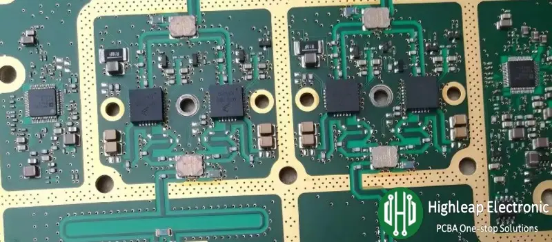
Understanding Silkscreen on PCB: A Comprehensive Guide for PCB Manufacturers

PCB Silkscreen
Introduction
PCBs form the essential infrastructure of modern electronics, providing a platform for the integration and interconnection of electronic components. While the functionality and electrical performance of a PCB are paramount, the aesthetic appeal and legibility of information on a PCB are equally significant. This is where the utilization of silkscreen becomes crucial. In this extensive guide, we will dive deep into the world of PCB silkscreen, exploring its significance, printing methods, design considerations, and much more.
What Is Silkscreen on PCB?
Silkscreen on PCBs is a layer of ink traces that has multiple purposes. It includes labels for various components, such as connector names, resistor and capacitor values, and other information, such as the title of the PCB, PCB production cycle number, PCB serial number, PCB panel position number, part polarity, and test point locations, which facilitate PCB traceability. This layer is usually applied to the component side of the printed circuit board, although it can also be applied to the solder side if required.
Apart from its practical benefits, the silkscreen also has a visual function. It can incorporate branding elements, company logos, and decorative features to enhance the overall appearance of the PCB, making it more appealing and professional. The ink used for the silkscreen layer is typically a non-conductive epoxy ink available in various colors such as black, white, red, blue, and yellow.
The silkscreen is a vital aspect of PCB design and plays a crucial role in the functionality of electronic circuits. Whether it’s a complex circuit designed by an engineer or a simple project assembled by a hobbyist, the silkscreen aids in the efficient assembly and troubleshooting of the circuit. It is positioned as the topmost layer of the PCB and serves as a reference for component placement, providing valuable information during the PCB assembly process. The ink used for silk screen printing on PCBs is specifically formulated with heat and chemical-resistant resins to withstand the soldering and assembly processes.

PCB is being silkscreen
Methods of Applying PCB Silkscreen
The choice of the silkscreen method depends on various factors, including time, cost, material, required accuracy, and board spacing. Here, we present three commonly employed PCB screen printing methods.
Manual & Automatic Screen Printing
Manual screen printing is considered the oldest and most cost-effective approach for PCB silkscreen printing. In this process, epoxy ink is manually applied to the laminate using a stencil, and then it is dried to achieve the desired impression on the PCB. One significant advantage of this method is its relatively simple setup requirements, making it a preferred choice for many applications. However, it is better suited for larger board sizes due to the larger text size associated with it, requiring sufficient space for the impression to dry effectively. If minimizing expenses and board spacing is not a constraint, manual screen printing is advisable.
Liquid Photo Imaging (LPI)
Liquid photo imaging involves coating the laminate with epoxy, which possesses photo imaging properties. The silkscreen design is then transferred to the board by exposing it to ultraviolet light through a photomask. LPI yields higher precision compared to manual screen printing and requires less space for implementation. However, it consumes more ink and setup time. When prioritizing PCB space conservation and achieving finer results, liquid photo imaging is the method of choice.
Direct Legend Printing (DLP)
Direct legend printing employs inkjet printers to transfer ink directly onto PCBs, similar to paper printers. This method allows for direct printing of CAD application information onto the board. It offers high accuracy and time efficiency, with a text height capacity as small as 0.02 inches. However, it is essential to avoid using text heights below 0.02 inches as they may be difficult to read. DLP is not suitable for PCBs made with silver materials, and there may be restrictions on the use of acrylic ink in certain cases.
Comparison of Silkscreen Techniques
| Silkscreen Technique | Manual Screen Printing | Liquid Photo Imaging (LPI) | Direct Legend Printing (DLP) |
|---|---|---|---|
| Process | Manual process using a stencil and squeegee to apply ink | Photographic process using a photosensitive emulsion and UV exposure | Inkjet printing directly onto the PCB |
| Precision | Moderate precision | High precision | High precision |
| Resolution | Limited resolution | High resolution | High resolution |
| Complexity | Requires skilled operator | Requires specialized equipment and chemical processes | Requires compatible inkjet printer and software |
| Time Efficiency | Moderate speed | Moderate to high speed | High speed |
| Setup Cost | Low | Moderate to high | Moderate |
| Text Height Capability | Moderate | Very fine | Very fine |
| Compatibility | Works with various PCB materials and ink types | Works with various PCB materials and ink types | May have limitations with certain PCB materials and ink types |
| Versatility | Suitable for low to medium volume production | Suitable for medium to high volume production | Suitable for low to medium volume production |
| Aesthetics | Can produce slightly rougher edges | Can produce sharp and precise edges | Can produce sharp and precise edges |
| Component Interference | Potential for interference if not carefully aligned | Minimal interference due to high precision | Minimal interference due to high precision |

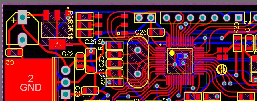
The is an example of an error in above picture
For boards with enough space on the PCB, when we design the PCB, the solder mask opening should generally be about 6.5 mil larger than the overall pad, and the character box should be about 3 mil larger than the window, because this will greatly facilitate the optimization of CAM engineers.
Benefits of Silkscreen Markings on PCBs
Component Identification
Silkscreen markings provide clear labels for components such as connectors, resistors, capacitors, and integrated circuits. These labels help users easily identify and locate specific components during assembly, testing, and troubleshooting processes.
Reference for Component Placement
Silkscreen markings serve as a visual guide for accurate component placement during PCB assembly. They indicate the designated positions for components, ensuring proper alignment and reducing the risk of errors or misplacements.
Improved Clarity and Readability
Silkscreen markings enhance the legibility of important information on the PCB. Clear and properly aligned text, symbols, and graphics make it easier for technicians, engineers, and users to interpret the board’s specifications, part numbers, reference designators, and other essential details.
Error Prevention and Quality Control
Silkscreen markings aid in error prevention and quality control during the manufacturing and assembly processes. By providing visual indicators, they assist in identifying any incorrect or missing components, reducing the likelihood of production errors, and improving overall product reliability.
Branding and Professional Appearance
Silkscreen markings can incorporate branding elements, company logos, and decorative designs onto the PCB. This enhances the professional appearance of the end product and increases brand recognition.
Enhanced Troubleshooting and Maintenance
Silkscreen markings facilitate troubleshooting and maintenance tasks by providing valuable information on component values, pin configurations, test points, and polarity markings. This enables technicians to quickly identify and address any issues, minimizing downtime and improving the overall efficiency of repairs.
Design Considerations for Silkscreen on PCBs
When designing the silkscreen for a PCB, several crucial factors need to be taken into account:
Size and Placement
The size of the silkscreen should strike a balance between readability and conserving space on the PCB. It should be large enough for easy readability without overwhelming the board. Additionally, the positioning should ensure clear visibility and avoid disrupting or obstructing other components.
Font and Style
Select a clear and legible font for the silkscreen text that is consistent throughout the PCB. Avoid using overly elaborate or complex fonts that may hinder readability.
Color
Carefully choose the color of the silkscreen. Dark colors like black or dark blue are generally easier to read, but the suitability may vary depending on the specific application or requirements.
Information
Include only essential information related to the circuit and its components on the silkscreen. Avoid redundant details or duplicating information already present elsewhere on the PCB to maintain clarity and avoid confusion.

The is an example of an error in above picture
PCB character optimization suggestions: If there are many characters to be optimized, the character attributes should not be copper attributes, otherwise it will be very troublesome to optimize the CAM engineering software. If the characters are dense, it is unavoidable to have characters on the pads and other problems. It is necessary to accept the fuzzy and incomplete characters and provide a clearer PDF for production.
Optimizing Silkscreen Character Design for PCBs
When designing silkscreen characters for PCBs, several key considerations ensure both functionality and clarity. Besides the character size, it’s essential to maintain a balanced height-to-width ratio, to ensure readability at various sizes. Characters should be positioned to avoid covering pads, vias, or traces, which can impact electrical performance and assembly quality. If characters must cross drill holes, partial obscuring is acceptable, but polarity marks should remain intact to prevent assembly and testing errors.
The choice of silkscreen color also plays a crucial role in readability and cost-efficiency. Unless specific color requirements exist, it’s advisable to use a single color for the silkscreen to reduce manufacturing costs. High-contrast colors like white on green PCBs enhance legibility, but if multiple colors are necessary, they should be chosen carefully to maintain clarity without significantly increasing costs.
Finally, providing a comprehensive PCB assembly diagram is vital. This diagram should clearly indicate the position and identification of all components, polarity markings, and critical test points. Detailed assembly instructions and guidelines ensure that the PCB is assembled correctly and efficiently. By adhering to these design principles, manufacturers can produce high-quality, functional, and easy-to-assemble PCBs.
Key Takeaways
Silkscreen on PCBs is a vital component of modern electronics, providing both practical and visual benefits. By carefully considering design aspects and employing appropriate silkscreen techniques, manufacturers can enhance the functionality, readability, and aesthetic appeal of PCBs. Highleap Electronic, a leading PCB manufacturer, understands the intricacies of silkscreen application and can help you save time and costs on your PCB projects. With our experience and manufacturing capabilities, we ensure precise silkscreen application and high-quality PCB production. Contact us today to see how our comprehensive PCB manufacturing services can benefit you.
Conclusion
In conclusion, silkscreen on PCBs is not just about aesthetic appeal but also plays a crucial role in ensuring the functionality and reliability of electronic circuits. By choosing the right silkscreen method and carefully designing the silkscreen layer, manufacturers can significantly improve the assembly, troubleshooting, and overall quality of PCBs. Highleap Electronic is committed to providing top-notch PCB manufacturing services, including precise and high-quality silkscreen application. Reach out to us for all your PCB needs, and let us help you achieve the best results for your electronic projects.
PCB Silkscreen FAQ
1.What are the common issues encountered with silkscreen alignment on PCBs?
Misalignment of silkscreen can occur if the printing process is not properly calibrated. This can lead to text and symbols being off-center, which may obscure important component pads or vias. Ensuring precise alignment during the setup process can help mitigate these issues.
2.How does silkscreen impact the manufacturability of a PCB?
Silkscreen provides clear labels and instructions that simplify the assembly process, reduce errors, and improve quality control. It enhances readability and helps in the accurate placement of components, thereby improving manufacturability.
3.What are the limitations of using silkscreen on high-density PCBs?
On high-density PCBs, space for silkscreen text is limited. This necessitates careful planning of text size and placement to avoid covering pads and vias. Advanced printing methods like Direct Legend Printing (DLP) can help achieve finer details in limited spaces.
4.Can silkscreen be applied to both sides of a PCB?
Yes, silkscreen can be applied to both the component side and the solder side of a PCB. This is particularly useful for double-sided or multi-layer PCBs where component identification and orientation are crucial on both sides.
5.How do environmental factors affect silkscreen durability?
Environmental factors such as humidity, temperature, and exposure to chemicals can impact the durability of silkscreen. Using high-quality, heat-resistant, and chemical-resistant inks ensures that the silkscreen markings remain legible and intact throughout the PCB’s lifecycle.

Take a Quick Quote