Back to blog
Why 16 Layer PCBs Are Essential for Advanced Electronic Designs

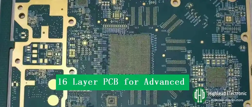
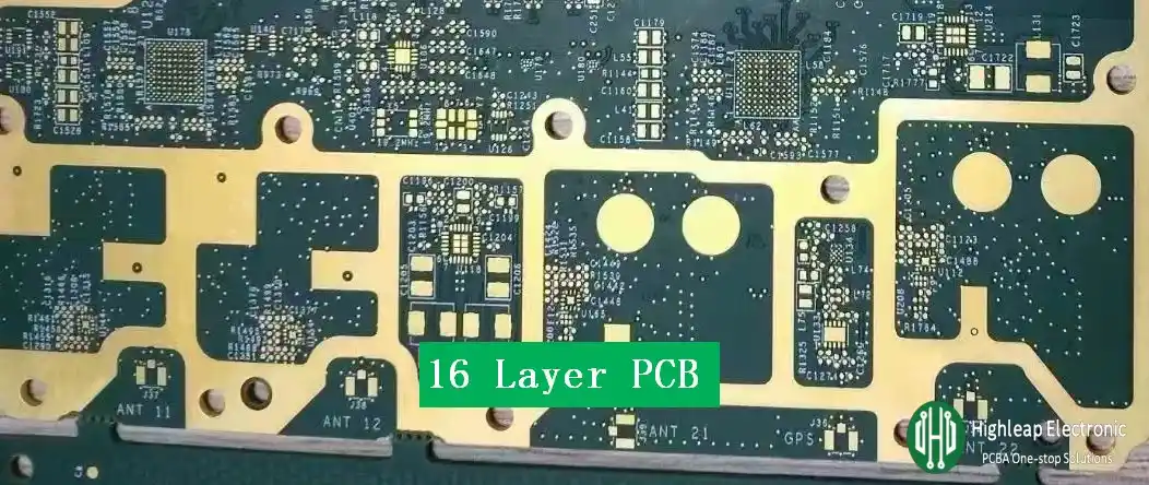
16 layer PCB for advanced electronics
16 layer PCB, which is critical for a wide range of applications such as advanced control systems, telecommunications and medical equipment. This comprehensive guide is designed to help procurement professionals gain an in-depth understanding of 16-layer PCBs and understand their structure, benefits, applications, design considerations and manufacturing processes.
Understanding 16 Layer PCB
The 16 layer PCB is composed of multiple PCBs laminated together. Therefore, the hole-to-line requirements are very strict for hole position tolerances and inter-layer alignment tolerances, so these aperture sizes and tolerances are very important for managing the complexity and high density of modern electronic designs. A typical 16 layer PCB stackup includes multiple routing, power, and ground layers, all carefully laid out to ensure optimal electrical performance, thermal management, and manufacturability. As a leading provider of 16-layer PCB manufacturing services, Highleap Electronic offers top-of-the-line – layered solutions for complex, high-speed and high-density applications.
Composition and Materials
The construction of 16 layer PCBs involves high-quality, halogen-free materials such as aluminum, CEM, and FR. The key components include:
-
- Prepreg Sheets: Fiberglass cloth coated with resin, acting as insulating materials between copper foil layers. Prepreg ensures proper insulation and minimizes signal interference.
- Copper Foil Sheets: These sheets serve as the primary conductive material, facilitating signal transmission and power distribution across the PCB.
- Laminate Sheets: These provide a substrate for bonding the copper layers, contributing significantly to the PCB’s functionality and performance.
The board thickness can extend up to 8 mm, with a maximum finished size of 500 x 500 mm, providing ample space for intricate circuitry and numerous components. It is recommended to use better PCB materials for high-rise PCBs, and do not only consider price and ignore the final product quality. Material selection can be viewed: PCB substrate materials.
Advantages of 16 Layer PCB Manufacturing
The 16 layer PCB offers numerous advantages that make it a preferred choice for high-performance applications:
-
- High-Density Interconnection (HDI): Supports complex electronic designs, making it ideal for advanced applications requiring multiple signal routing layers.
- Superior Signal Integrity: Efficient signal routing minimizes signal loss and electromagnetic interference, ensuring reliable performance.
- Enhanced Functionality: Accommodates more components and circuitry within a compact design, enhancing device functionality.
- Space Efficiency: Reduces the overall size of electronic devices, making it suitable for space-constrained applications.
- Lightweight Design: By eliminating connectors for separate PCBs, 16-layer boards contribute to a lighter device construction.
- Increased Durability: Multiple layers of insulation and bonding materials enhance the robustness and longevity of the PCB.
Applications of 16 Layer PCBs
The advanced capabilities of 16 layer PCBs make them indispensable in a wide array of industries. Notable applications include:
-
- Satellite Systems
- Industrial Controls
- GPS Technology
- Telecommunications
- Computer Systems
- Medical Equipment
- Test Equipment
- Meteorological Systems
- Nuclear Detection Systems
- Atomic Accelerators

16 Layer PCB
Layer Planning Guidelines for 16-Layer PCBs
Effective layer planning is essential for optimizing the performance of 16 layer PCBs. A symmetric distribution of layers is key, splitting them evenly between the top and bottom to prevent warping and ensure symmetry. Ground and power distribution should be allocated carefully, with at least 20% of the layers dedicated to each, leaving the remaining 60% for signals. Controlled impedance can be achieved by placing ground and power layers adjacent to signal layers, which also aids in decoupling.
Additionally, heat dissipation is improved by positioning ground layers on the outermost parts of the board, facilitating easier routing. Uninterrupted ground planes are vital, so it’s recommended to assign a full ground plane layer on each side adjacent to signal layers. Split power planes should be defined to isolate different power domains such as analog, digital, and high-current. Finally, signal layers should be ordered for optimized grouping based on the specific needs of high-speed, RF, or isolated sections of the system.
Key Design Considerations for 16-Layer PCBs
When designing a 16 layer PCB, several key points must be considered:
-
- Via Technology: Laser-drilled microvias with approximately 0.2mm holes allow dense interconnections between layers. Backdrilling clears unused sections of vias.
- Routing Channels: Thinner dielectrics like 0.008″ prepregs between layers provide adequate trace routing channels.
- Controlled Impedance: Ground and power layers adjacent to signal layers allow impedance control for high-speed traces.
- Decoupling: Multiple power-ground pairs spread across layers provide decoupling capacitors access.
- Thermal Management: Thermal reliefs and thermal core layers help conduct heat away from inner layers.
- Signal Integrity: Follow length matching, tuning, and crosstalk guidelines for high-speed traces.
- Manufacturability: Work closely with the fabricator early to check design for manufacturability (DFM), panel utilization, and fabrication tolerances.
A disciplined approach is needed when laying out complex 16 layer designs, with close collaboration with the PCB manufacturer to ensure producibility.
Fabrication and Testing Considerations
During the fabrication and testing of densely packed 16-layer boards, the following considerations are critical:
-
- Registration Accuracy: Ensuring drilled holes match pads across 16 layers when stacking up.
- Layer Alignment: Precise alignment over large board sizes typical of high-layer-count PCBs.
- Heat Dissipation: Uniform heat dissipation across the multilayer stackup requires careful processing during lamination.
- Plating Quality: Strict control of plating quality and hole wall profiles for reliable interlayer connections.
- Electrical Testing: Extensive electrical test coverage due to the high node count on large multilayer boards.
- Advanced Testing: Impedance control, signal integrity, and RF performance testing require advanced test equipment.
The fabrication facility must have proven experience in manufacturing complicated high-layer-count PCBs cost-effectively. The manufacturing facility must have proven experience in manufacturing complex multi-layer PCBs in a cost-effective manner. For this kind of complex multi-layer PCB, it is recommended to carry out tolerance control on holes and hole position tolerances. In particular, the tolerances of crimping holes should be controlled more strictly. The manufacturer should be reminded of these tolerances.
Recommendations When Ordering
To ensure the successful manufacturing of 16 layer PCBs, consider the following recommendations:
-
- Experienced Fabricator: Partner with a fabricator experienced in building 16+ layer PCBs.
- Pre-DFM Analysis: Request pre-DFM analysis before finalizing the layer stackup.
- Prototyping: Have quick-turn prototypes made to validate the design and process before committing to production.
- Capability Understanding: Understand the fabricator’s capabilities regarding layer tolerance, hole size ranges, line/space specifications, etc.
- Thermal and Signal Integrity Validation: Discuss any thermal design and signal integrity validation needs.
- Test Coverage Review: Review test coverage requirements, including bare board electrical testing, flying probe testing, and in-circuit testing (ICT).
- Panel Optimization: Get recommendations for optimal panel sizes, layout, and breakout.
Conclusion
A well-planned layer stackup strategy is crucial for effectively utilizing the routing real estate available in 16-layer designs. The layer sequence must balance signal routing needs, power distribution, heat dissipation, and manufacturability constraints. A collaborative approach between the designer and fabricator ensures a practical stackup optimized for cost, quality, and performance. Rigorous design reviews and testing will validate the complex multilayer implementation before volume production.
For procurement specialists, understanding the intricacies of 16-layer PCBs is essential. Highleap Electronic stands out as a leading manufacturer, delivering top-tier quality and precision in 16 layer PCB production. Contact us today to discuss your project requirements and experience the Highleap Electronic difference.
Related Articles
Understanding Field-Effect Transistors (FETs) in PCB Design
Dive into the fundamentals of Field-Effect Transistors (FETs) and their critical role in PCB design.
Future Prospects and Challenges in Local Oscillator Development
Developing multi-function chips that integrate local oscillators(LOs) with other RF components, such as mixers, amplifiers, and filters, is an emerging trend.
Common Anode and Common Cathode 7 segment displays
This comprehensive guide delves into the intricacies of 7-segment displays, their types, functionalities, and design considerations in PCB layouts.
Take a Quick Quote


