
Back to blog
Key Considerations in High-Frequency RF Board Design

RF Boards
Introduction
In today’s rapidly advancing world of electronics, RF boards and microwave PCBs are pivotal in driving innovation. These specialized components underpin a plethora of cutting-edge technologies, from 5G networks and satellite communications to advanced radar systems. As frequencies escalate and signal integrity grows more crucial, mastering RF board design has never been more pivotal.
This comprehensive guide delves deep into the nuances of RF and microwave PCB design, offering invaluable insights for engineers, designers, and technology enthusiasts alike. We’ll explore advanced techniques, common pitfalls, and emerging trends that are shaping the future of high-frequency circuit design.
Understanding RF and Microwave Boards
Before diving into advanced topics, it’s essential to establish a solid foundation by defining what makes RF and microwave boards unique:
Frequency Range:
-
- RF boards typically operate between 300 kHz and 300 GHz.
- Microwave boards focus on frequencies from 300 MHz to 300 GHz.
Critical Characteristics:
-
- Low signal loss
- Precise impedance control
- Minimal crosstalk and EMI
- Compatibility with high-frequency materials
Applications:
-
- Wireless communications
- Radar systems
- Satellite technology
- Medical imaging equipment
- Test and measurement instruments

Radio Frequency circuit board with components assembled
Key Considerations in RF Board Design
Material Selection
The choice of board substrate plays a pivotal role in RF design. Unlike standard FR-4 used in lower frequency applications, RF boards often necessitate specialized materials:
- Rogers RO4350B: Excellent for frequencies up to 10 GHz
- Rogers RT/duroid 5880: Ideal for millimeter-wave applications
- PTFE (Teflon) based materials: Low dielectric constant and loss tangent
Factors to Consider:
- Dielectric constant (Dk)
- Dissipation factor (Df)
- Thermal stability
- Cost-effectiveness
Impedance Control
Maintaining consistent impedance throughout the RF signal path is critical:
- Common impedances: 50Ω for most RF applications, 75Ω for some video and cable TV systems
- Utilize impedance calculators and field solvers for accurate trace width calculations
- Consider microstrip and stripline configurations for varying layer requirements
Transmission Line Design
Proper transmission line design is essential for preserving signal integrity:
- Microstrip: Simplest to design, but more susceptible to external interference
- Stripline: Offers better isolation, but is more complex to implement
- Coplanar waveguide (CPW): Provides a balance of performance and ease of manufacturing
Grounding and Power Distribution
Effective grounding is crucial in RF board design:
- Implement solid ground planes
- Use stitching vias to connect ground planes on different layers
- Consider ground pour techniques for top and bottom layers
Component Placement and Routing
Strategic component placement significantly impacts RF performance:
- Keep signal paths as short as possible
- Utilize ground vias near RF components for improved isolation
- Implement guard traces and ground fences for sensitive signals
EMI/EMC Considerations
Electromagnetic interference (EMI) and electromagnetic compatibility (EMC) are critical considerations in RF design:
- Use shielding techniques for sensitive circuits
- Implement proper stack-up design to minimize radiation
- Consider edge plating to reduce edge radiation
Advanced RF Board Design Techniques
3D Electromagnetic Simulation
Utilize advanced EM simulation tools to optimize designs:
- ANSYS HFSS
- CST Microwave Studio
- Keysight ADS
These tools enable:
- Visualization of field distributions
- Optimization of antenna designs
- Analysis of complex multi-layer structures
Distributed Element Design
At high frequencies, distributed element design offers an alternative to traditional lumped elements:
- Replace inductors with high-impedance lines
- Use low-impedance, wide traces as capacitors
- Implement quarter-wave transformers for impedance matching
RF-Specific Component Considerations
When selecting components for RF boards, factors to consider include:
- Q-factor of inductors and capacitors
- Self-resonant frequency (SRF) of passive components
- Package parasitics and their impact on performance
Advanced Stackup Techniques
Optimize board stackup for RF performance:
- Implement buried striplines for critical signals
- Use selective via antipads to control impedance
- Consider hybrid stackups with both FR-4 and high-frequency materials
Thermal Management in RF Boards
High-frequency circuits generate significant heat:
- Use thermal vias under power amplifiers and heat-generating components
- Consider embedded heat sinks in multi-layer designs
- Implement proper copper balancing for even heat distribution
Signal Integrity in Mixed-Signal RF Designs
When integrating RF and digital circuits:
- Use proper partitioning to isolate RF and digital sections
- Implement separate power planes for RF and digital supplies
- Consider the use of blind and buried vias to minimize crosstalk
Advanced Manufacturing Techniques
Leverage cutting-edge manufacturing processes:
- Laser-drilled microvias for high-density interconnects
- Sequential lamination for complex multi-layer designs
- Embedded passives to reduce parasitics and improve performance
Emerging Technologies in RF Board Design
Stay ahead with these emerging trends:
- Considerations in 5G and mmWave board design
- Substrate Integrated Waveguide (SIW) technology
- Additive manufacturing for RF components

Radio Frequency PCB with components assembled
Navigating Common CAM Challenges in RF Board Manufacturing
CAM engineers frequently encounter design challenges when manufacturing RF PCBs. The main characteristics of RF PCBs, such as dense traces, complex solder mask openings, and intricate via processes, pose significant difficulties. Ensuring complete connectivity of the circuit network without short circuits, precise via filling processes, and maintaining integrity in character designs are crucial for CAM engineers. These aspects significantly alleviate the complexity of preparing Gerber files.
These challenges underscore the importance of collaboration between CAM engineers and PCB designers to adhere strictly to design guidelines. Advanced tools for design verification and simulations are instrumental in identifying and resolving potential issues early in the design phase. This proactive approach optimizes trace spacing, minimizes crosstalk, and ensures precise alignment between PCB layers.
Furthermore, CAM engineers must address issues related to insufficient solder mask clearances and inaccuracies in drill registrations. Utilizing CAM software with tailored design rule checks (DRC) for RF applications is essential. By optimizing these parameters, CAM engineers can improve PCB yield rates and streamline the manufacturing process. Incorporating thorough DFM reviews and maintaining effective feedback loops between CAM and design teams are critical to achieving robust RF PCB designs that meet stringent performance requirements.
Conclusion
Mastering RF board design is a journey of continuous learning and adaptation. As frequencies rise and applications become more demanding, staying updated with the latest techniques and technologies is imperative. By implementing the advanced strategies outlined in this article, designers can create high-performance RF boards that meet the rigorous standards of modern wireless communications and beyond.
Remember, successful RF PCB design blends art and science. It demands a profound understanding of electromagnetic principles, material properties, and manufacturing processes. Continuous experimentation, simulation, and prototyping are crucial for achieving optimal results.
Looking forward, the field of RF board design will continue evolving. From the advent of 6G technologies to further exploration into millimeter-wave and terahertz spectrums, and the integration of RF with advanced digital and optical systems, new challenges and opportunities for innovation will emerge.
Discover more about cutting-edge RF board solutions at Highleap Electronic.
FAQs
What role does environmental resilience play in RF board design?
Environmental resilience refers to the board’s ability to withstand harsh conditions such as extreme temperatures, humidity, and mechanical stresses. Ensuring robust environmental resilience involves selecting materials with high thermal stability, employing effective sealing techniques, and designing for reliability in challenging operational environments.
How do electromagnetic compatibility (EMC) regulations impact RF board design?
EMC regulations govern the permissible levels of electromagnetic interference emitted by electronic devices. Compliance requires careful consideration of shielding effectiveness, layout optimization to minimize emissions, and adherence to specific emission limits across different frequency ranges. Addressing EMC early in the design phase ensures regulatory compliance and enhances product reliability.
What are the implications of component miniaturization on RF board design?
Miniaturization trends in electronics necessitate compact RF board designs without compromising performance. This entails utilizing advanced manufacturing techniques like microvias for dense interconnects, optimizing component placement for minimal signal loss, and integrating high-frequency materials that support miniaturized designs while maintaining signal integrity and thermal management.
How does supply chain resilience impact RF board manufacturing?
Supply chain resilience refers to the ability of manufacturers to adapt and recover swiftly from disruptions such as material shortages, geopolitical instability, or natural disasters. Mitigating risks through diversified sourcing, maintaining strategic inventory levels, and fostering collaborative relationships with suppliers are critical strategies for ensuring uninterrupted production and timely delivery of RF boards.
What advancements are driving the future of RF board integration with AI and IoT technologies?
Integration of RF boards with artificial intelligence (AI) and Internet of Things (IoT) technologies is expanding applications in smart cities, autonomous vehicles, and industrial automation. Innovations include AI-driven adaptive RF systems for real-time optimization, IoT-enabled RF sensors for predictive maintenance, and scalable architectures that facilitate seamless integration into interconnected ecosystems.

Related Articles
What is EMI, EMS and EMC?
At Highleap Electronic, we specialize in producing high-quality PCBs by integrating advanced techniques for impedance control, ensuring robust EMC and mitigating EMI.
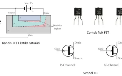
Understanding Field-Effect Transistors (FETs) in PCB Design
Dive into the fundamentals of Field-Effect Transistors (FETs) and their critical role in PCB design.

Future Prospects and Challenges in Local Oscillator Development
Developing multi-function chips that integrate local oscillators(LOs) with other RF components, such as mixers, amplifiers, and filters, is an emerging trend.
Take a Quick Quote