
Back to blog
5G Impact on PCB Manufacturing: Challenges & Opportunities

Introduction
One sector that will undoubtedly face disruption is printed circuit board (PCB) manufacturing. As the core electronic component in virtually all 5G-enabled devices, PCBs must evolve to support the technical demands of this new wireless standard. Meanwhile, PCB producers must adapt their design, material, and production processes to satisfy the growth in 5G device demand.
This article provides an in-depth examination of how 5G is impacting the PCB manufacturing industry. We’ll explore the technical capabilities of 5G networks, analyze the changes they necessitate for PCB design, and outline both the challenges and opportunities emerging for PCB manufacturers. The goal is to illuminate the profound and wide-ranging effects 5G adoption will have on this crucial segment of the global electronics supply chain.
What is 5G Technology?
Before delving into 5G’s impact on PCBs, it’s important to understand the technological advances powering this new wireless generation. Known as the fifth generation of cellular mobile communications, 5G networks offer unprecedented speeds, ultra-low latency, and vast improvements in connectivity.
Specifically, 5G networks operate using one of three spectrum bands – low, mid, or high frequency – to deliver the following key enhancements over 4G LTE networks:
- Speed: 5G peak download speeds are projected to reach 20 Gbps, over 20x faster than 4G’s 1 Gbps maximum. Real-world speeds should average 100 Mbps-1 Gbps with latency under 10 milliseconds.
- Latency: The reduced latency of 5G – transmission delays as low as 1 ms – enables applications requiring near instant response times like autonomous vehicles, remote surgery, and VR/AR.
- Connectivity: Greater bandwidth allows 5G to connect many more devices simultaneously with reliable, high-quality links even in dense, crowded conditions.
- Reliability: Thanks to network slicing, specific industries like manufacturing can benefit from dedicated ultra-reliable low latency connectivity ideal for mission-critical applications.
- Coverage: Additional high-frequency spectrum gives 5G the ability to transmit small cell coverage in a fraction of the physical space required by previous standards.
Clearly, 5G offers transformative capabilities that will drive new use cases across industries. However, realizing its full potential requires network infrastructure and compatible user devices – including advanced PCBs.
The Evolving Role of PCBs in 5G Devices
Traditionally, PCBs serve as the foundation and interconnect layer for electronic components inside devices. However, the integration of multiple new 5G technologies necessitates several alterations to standard PCB design paradigms.
Broadly, the shift from 4G to 5G demands:
- Smaller, thinner, higher-density PCBs to fit expanded 5G chips and antennas into increasingly compact form factors
- Greater RF performance from lower-loss, higher-speed materials to withstand 5G’s wider bandwidth and channel sizes
- Improved thermal management to dissipate heat from powerful 5G modem/RF modules operating across wider bandwidths
More specifically, key changes to PCB composition and construction include:
- Embedded Multi-Antenna Array Designs: Integrating several antenna elements directly into multilayer PCB boards to minimize interconnect losses and space demands.
- RF/Digital Co-Design: Combining RF and digital/baseband circuitry onto the same PCB substrate for tighter integration and synchronization instead of separating into modules.
- Increased Circuit Density: Adopting fine-line (<20um) trace widths and miniaturized passive components to fit more functionality in less space using advanced fabrication techniques like selective plating.
- Thermally Conductive Core Materials: Replacing standard FR-4 with composites containing ceramics, carbon fiber, or graphene to draw heat away from concentrated heat sources.
- mmWave Circuitry: Designing transmission line structures optimized for millimeter wave 5G spectrum bands through novel dielectric materials.
Clearly, next-generation PCBs integrating these advanced designs and materials have become critical in realizing the true capabilities of 5G technology.
Why 5G Matters for PCBs
The technological feats 5G makes possible have major implications for PCB design approaches and production processes. Existing 4G PCB implementations separate radio and baseband functionality across discrete modules connected by fiber or copper traces. In contrast, true 5G integration demands more unified, higher density solutions. Some key ways 5G is reshaping PCB priorities include:
- Antenna Design: 5G networks employ array antennas using multiple active elements to direct highly focused beams for coverage and capacity. This shifts antenna implementation from standalone modules to directly embedding complex antenna arrays directly into PCB multilayer builds.
- Edge Computing Integration: 5G enables distributing processing power to network edges via concepts like Mobile Edge Computing (MEC). PCBs must integrate diverse chips hosting edge applications, from baseband processors to AI accelerators, adding thermal, electrical and mechanical complexity.
- Miniaturization: Size constraints from shrinking consumer devices demand ever smaller, thinner PCBs packed with more critical components. 5G circuitry must fit in tight footprints without sacrificing functionality or incurring signal integrity issues.
- Thermal Management: Higher output mmWave signals generate more heat, as do denser multi-core SoCs powering edge applications. Dissipating this extra thermal load within compact enclosures requires advances in conductive and convective cooling at the PCB level.
- Connectivity Support: 5G systems leverage multiple simultaneous connectivity methods including mmWave, sub-6GHz, WiFi, and Bluetooth. Unifying diverse high-speed interfaces within limited real estate brings electrical and RF challenges.
- Automation: Producing these intricate 5G-capable boards at volume requires sophisticated fabrication, assembly, and inspection solutions optimized for product reliability, yield, and throughput.
Keeping pace with 5G demands rethinking traditional PCB design approaches and production methodologies. Those able to rapidly iterate and refine their solutions will be best positioned long-term as networks advance and myriad new applications emerge.
How 5G Affects Manufacturing Considerations
Anticipating and responding to the design changes 5G necessitates means proactively addressing impacts across PCB manufacturing processes and facilities. Key production areas set to evolve include:
Materials Innovation
With higher frequencies come greater power losses as signals propagate through board laminates. New ceramics, composites and additive substances possessing ultra-low dielectric constants help minimize path attenuation for mmWave circuits, often less than 2 for certain applications. Alternative thermally conductive yet flexible substrates also enable designs unfeasible just years ago. Continuous materials R&D remains essential as 5G standards progress.
Design Methodologies
Traditional subtractive PCB manufacturing struggles with 5G’s minuscule lines and gaps below 100 microns. Fabricators increasingly rely on semi-additive processes like copper-filled laser drilling to produce tight-tolerance microvias and traces critical for antenna and high-speed digital designs. 3D component embedding and conformal shielding using technologies like direct metallization further augment functionality.
Thermal Engineering
Advanced computational modeling quantifies heat flow under varied usage profiles. Techniques like fused deposition modeling then produce strategically embedded heatsinks addressing localized hotspots. New gap filler formulations like anisotropic adhesives transfer waste away from sensitive electronics more effectively as well. Thermal assurance remains paramount with rising wattage densities.
Miniaturization Techniques
Tiny compound antenna arrays required for mmWave link establishment stretch current assembly capabilities. Fabricators employ cutting-edge approaches including sequential lamination, wafer-level processing and 3D printer-compatible designs to reliably build intricate multi-layer structures within a few square millimeters. Component miniaturization similarly progresses via new heterogenous integrations.
Production Workflow Optimization
Leveraging automated optical inspection and inline metrology helps identify defects earlier when manufacturing miniature multi-cavity boards with narrow safety margins. Data analytics further aid continuous improvement by revealing bottlenecks and informing predictive maintenance. Advanced cleanrooms maintain stringent contamination controls for nanoscale work.
Quality Monitoring
Stringent radio frequency testing regimes leverage specialized anechoic chambers and network analyzers to thoroughly vet 5G devices for compliance, efficiency and performance under real-world conditions. Beyond functional testing, advanced failure analysis gives deeper insight into reliability issues like cracked solder joints or delamination under thermal stresses. Comprehensive quality remains a non-negotiable necessity.
Facility Modernization
Accommodating next-gen methodologies may require additional clean production space, specialized tooling and rigorous change control. Strategically located regional factories also assist timely low-volume customizations and prototype runs. Efficient floorplans minimize material waste while swift outfitting keeps pace with rapid technological shifts. Adaptability remains a long term competitive differentiator.
When the project moves from research to an RFQ, review RF PCB fabrication and SMT PCB assembly so the material, process, and inspection requirements stay aligned.
The Challenges and Opportunities of 5G
While 5G introduces several technical hurdles, proactive manufactures can harness it to strengthen their businesses for years ahead, provided they take a forward-looking perspective:
Challenges:
- Complex multi-functional designs strain assembly yields
- Miniscule tolerances necessitate nanometer precision fabrication
- Advanced materials research requires extensive R&D investments
- Ensuring reliable thermal dissipation across varied form factors
Opportunities:
- First-to-market advantages by enabling new 5G applications
- Accessing booming demand from consumer, industrial and infrastructure segments
- Developing core competencies in areas like antenna integration and heterogeneous packaging transferable to future technologies
- Strategic investments building resources position companies for long term leadership
- Facilities able to support both high-volume production and bespoke quick-turn prototypes command pricing premiums
For manufacturers proactive in overcoming hurdles, the future remains bright. Projections forecast the global PCB market reaching $74.1 billion by 2027 as 5G proliferates across industries, with Asia Pacific anticipated to lead growth (Grand View Research, 2021). Those optimized for 5G will emerge well positioned to not only capture initial expansion, but retain relevance as standards continue to progress. Continuous learning and refinement remains paramount in a field undergoing constant paradigm shifts.
Conclusion
5G represents the dawn of a new generation of connectivity delivering capabilities enabling countless as-yet unforeseen applications. While introducing tremendous complexity, it also presents the PCB industry a prime opportunity to both drive and benefit from this wave of innovation through foresight, flexibility and partnership.
Manufacturers embracing change by thoughtfully evolving their materials, processes, people and facilities today help light the path towards a seamlessly connected 5G future. Those unwilling or unable to adapt risk being left behind as networks and technologies march ever onwards. The coming years promise tremendous transition – for innovators actively shaping this revolution, the rewards are sure to be great.

Related Articles

LED High Bay Light PCBs: Metal-Core Light Engines, Drivers & Turnkey Boards Built to Spec
Get LED high bay light PCB fabrication and assembly for metal-core engines, drivers, surge boards, sensors and industrial lighting programs.
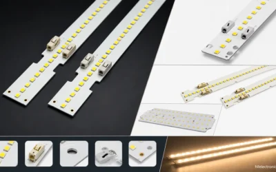
LED Linear & Strip Light PCBs: Long-Format Engines, Flexible & Rigid-Flex Boards
Build LED linear light PCBs for long rigid boards, flexible strips, rigid-flex lighting engines, RGBW control and even current distribution.
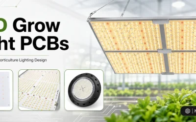
LED Grow Light PCBs: Multi-Channel Spectrum Boards, Drivers & Thermal Design
Manufacture LED grow light PCBs for full-spectrum engines, multi-channel drivers, thermal control boards and horticulture lighting assemblies.