
An In-Depth Guide to PCB Functional Testing

Introduction
Printed circuit boards (PCBs) are at the heart of almost every electronic product today. They provide the foundation for mounting and interconnecting components to bring a system design to life. While PCBs may appear simple, they involve sophisticated design, fabrication and assembly processes.
This results in extremely complex and dense boards that demand thorough testing to ensure quality and reliability. PCB functional testing is one such critical procedure performed on fully assembled boards to validate their functionality.
This guide takes an in-depth look at PCB functional testing – its meaning, methods, tools, importance and role in the manufacturing workflow. For design engineers and quality managers working on electronic products, it is essential to have a sound grasp of functional testing principles and practices.
What is PCB Functional Testing?
Functional testing refers to systematically checking populated printed circuit board assemblies (PCBAs) to confirm that the boards perform their intended functions correctly.
It involves stimulating the inputs of the assembled board in a manner that simulates its real operating conditions and monitoring the outputs. The input stimuli and output responses are then compared to the expected functional behavior of the board.
Functional testing is focused on validating the overall performance and operation of a fully assembled board. It goes beyond component-level or bare board testing to examine the PCB as a functioning system.
The aim is to catch any defects or issues that may have escaped earlier testing, and ensure the boards operate reliably as per the specifications before shipment. This provides a final product quality check at the end of the manufacturing process.
Why Perform Functional Testing on PCBs?
While PCBs do undergo various intermediate tests during fabrication and assembly, functional testing provides unique and essential benefits:
Validates overall board functionality: Earlier PCB tests like in-circuit test (ICT) focus on components. Functional testing verifies the complete board functions properly.
Catches assembly defects: Faulty solder joints, misplaced parts etc. may evade detection earlier. Running boards at operating loads/conditions highlights these.
Confirms design correctness: The test validates that the PCB meets all design parameters, performances and circuit requirements.
Emulates operating conditions: Stimulating inputs and monitoring outputs under near-real usage conditions ensures the board will function correctly in the field.
Prevents field failures: Defective boards identified through functional testing are fixed or scrapped, preventing premature field failures and saving after-sales costs.
Provides design feedback: Any functional issues found help improve the board design, assembly process and component selections for future builds.
Thus, functional testing is the final quality and reliability check performed on manufactured boards before shipment to customers. It is an essential step in the PCBA production workflow.
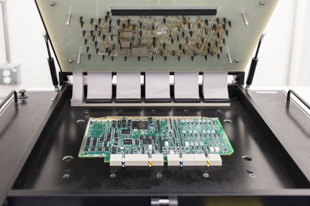
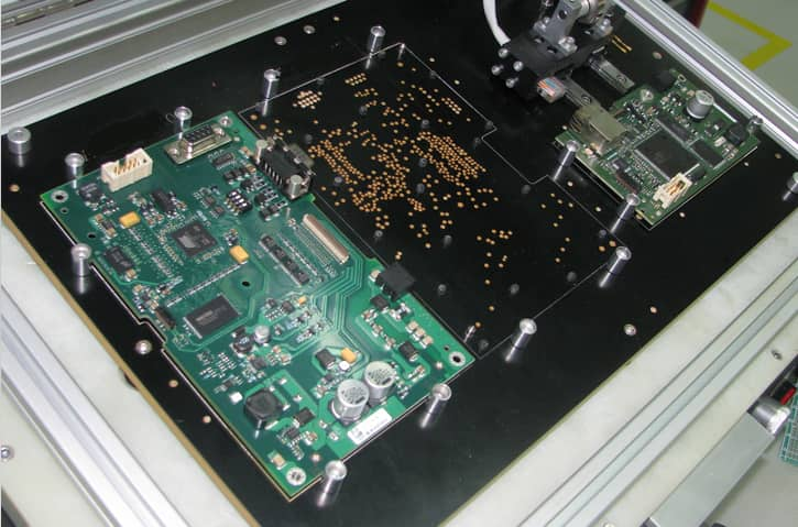
PCB Functional Testers
Dedicated functional test equipment is used to perform PCB functional testing in a systematic and automated manner. A functional tester consists of:
- Test Fixture – A custom mechanical fixture designed to securely hold the PCB under test and appropriately connect the required test points on the board to the tester.
- Interface – The electromechanical interface makes contact with test nodes on the board. Popular interfaces include “bed-of-nails” pins or flying probe test heads.
- Signal Sources – These generate the electrical stimuli to the board, simulating inputs in actual operating conditions. Common sources include function generators, power supplies etc.
- Measurement Equipment – Instruments like oscilloscopes, multimeters etc. connected to tester channels to measure PCB outputs.
- Switch Matrix – Switches route signals from sources to PCB inputs and responses from PCB to measurement equipment.
- Test Program – Software that coordinates the tester hardware and executes the automated test sequence based on the specific board’s design.
- PC and Display – A computer runs the test software while a display shows results and test reports.
Some testers provide features like boundary scan and JTAG testing capabilities too for programming and debugging boards. High-end testers integrate multiple test instruments in a single platform to provide complete PCB testing functionality.
PCB Functional Test Methods
There are a variety of functional test techniques used by PCB manufacturers:
Power-On Testing
The bare minimum way to functionally test a board is to simply power it up and check if onboard components like LEDs, displays, fans work as expected. This provides a quick initial go/no-go test but lacks thoroughness.
Manual Testing
Boards are manually operated in real-life conditions and output waveforms visually checked on oscilloscopes. While this can test functionality, it depends heavily on the skill of the tester.
Automated Testing
This employs a dedicated tester setup. Programmed input signals stimulate the PCB while outputs are captured and analyzed to check for correctness. Fully automated process.
Burn-In Testing
Running populated boards for prolonged periods at elevated voltages and temperatures to filter out latent defects and early failures. Provides an accelerated life test.
Margin Testing
Involves testing the board at operating extremes beyond nominal conditions to check functionality and design margins. Useful for safety-critical applications.
Regression Testing
Re-running a previously performed functional test again after design changes or rework to ensure existing functionality has not been impacted.
In-Circuit Emulation
Uses emulator probe hardware that targets test points. Emulators simulate connected chips like microcontrollers without needing the actual components populated.
For maximum defect coverage and reliability assurance, a combination of testing approaches may be applied to exercise the boards thoroughly.
Implementing PCB Functional Testing
To implement functional testing properly, PCB manufacturers need to factor in these considerations:
Test Coverage – Define test coverage metrics like the percentage of board nets or components terminals functionally verified to meet quality goals.
Test Access – Incorporate test points, vias and other design-for-test (DFT) provisions for tester access during layout.
Test Fixture – Design custom fixtures specific to the board geometry to interface securely with the tester.
Test Program – Develop software to automatically run simulations and verify board behavior based on schematics/netlists.
Diagnostics – Tools to isolate the root causes and failure mechanisms when boards fail the functional test.
Traceability – Systems to link results back to fabrication processes and individual PCB serial numbers for quality tracking.
Process Integration – Incorporate functional testing at relevant points within manufacturing process flows for completing boards.
Statistical Process Control – Apply statistical methods like capability indices to monitor functional test performance and make data-driven improvements.
Optimization – Refine testing routines regularly to reduce cycle times or improve test coverage. Utilize parallel testing where possible.
With careful planning, functional testing can be smoothly integrated within manufacturing lines without throughput impacts.
Role of Functional Testing in The PCB Production Workflow
Functional test complements the suite of verification steps implemented through the fabrication, assembly and integration process:
Design Verification – Simulate and optimize the PCB design upfront using SPICE models before prototyping.
Prototype Testing – Build and test engineering prototypes to confirm functionality before commencing volume production.
Bare Board Testing – Test unpopulated boards for defects like shorts, opens, impedance errors.
In-Circuit Testing – Check individual component placements and solder joints after population by electrical probing.
Board Interconnect Testing – Examine die-to-board wire bonds/solder balls in packaged ICs for defects.
Boundary Scan Testing – Use boundary scan cells to isolate faults and verify board wiring.
Point-to-Point Testing – Check continuity between test points to capture assembly errors.
Functional Testing – Validate overall board functionality under electrical operating conditions.
Burn-In Testing – Operate boards for extended durations to precipitate infant mortality failures.
System Integration – Test PCB performance when integrated within the complete system.
Thus, functional testing provides the final performance and reliability screening stage before boards get integrated into end products.
Benefits of Automated Functional Testing
While manual functional testing is possible for simple boards, automated testing using a fixture brings important benefits:
Repeatability – Eliminates variability from manual testing and provides consistent stimulus conditions.
Versatility – Test systems can be programmed to functionally test a wide range of different boards.
Scalability – Parallel test heads allow running batches of boards simultaneously for high throughput.
Accessibility – Fixtures enable probing densely packed boards where manual access is difficult.
Continuous monitoring – Critical parameters can be monitored continuously during testing versus intermittent manual checks.
Reliability – Automated testing prevents human errors and oversight.
Traceability – Results include time stamps and records for analyzing failures.
Diagnostics – Automated routines can precisely identify faulty nets or components for diagnosis.
Optimization – Test coverage, sequences and limits can be refined based on results to optimize effectiveness.
Data collection – Large volumes of test data can be aggregated and mined to derive manufacturing insights.
Thus, automated functional testers, though requiring upfront investment, pay dividends through higher quality, yield and reliability.
Functional Testing vs In-Circuit Testing for PCBs
PCB functional testing is sometimes mistaken to be the same as in-circuit testing. While both check populated boards, some key differences exist:
- Stage – ICT is done during manufacturing, while functional testing is done on finished boards.
- Scope – ICT checks individual components while functional testing verifies overall board operation.
- Stimulus – ICT uses bed-of-nails to probe nets. Functional testing provides real input signals.
- Configurability – ICT has fixed pin configurations. Functional testing uses programmable instruments.
- Coverage – ICT accesses limited test nodes based on fixture design. Functional testing can target required nodes.
- Diagnostics – ICT mainly detects assembly issues like missing parts or bridges. Functional testing reveals board performance issues.
- Failures caught – ICT finds defects arising from SMT and manual assembly. Functional testing catches design flaws too.
Thus, while ICT focuses on assembly quality, functional testing provides design verification and performance validation. The two approaches complement each other in the manufacturing chain.
Functional Test Fixtures for PCBs
Functional test fixtures secure the board and provide the electrical interface to the tester hardware. Key aspects that need consideration during fixture design are:
Interface – Needle probes, spring probes or pogo pins are commonly used to contact test nodes on boards. Zero insertion force connectors allow mating the fixture without applying excessive force on boards.
Signal routing – Short electrical connections between the interface points, switch matrix and measurement equipment using cabling, pcb backplanes or links embedded within the fixture body.
Node access – Ensure adequate clearances and openings in the holding structure for interfacing test probes with all required nodes on the board top and bottom sides.
Secure holding – Use clamps, brackets, vices and stops to hold boards firmly during handling and testing.
Registration – Precisely locate boards in space and align interface points using fixtures pins, guides, holes and datum surfaces.
Interchangeability – Quick-change modular components allow reconfiguring fixtures easily for different board types.
Durability – Use rigid, non-deforming materials like metals and advanced polymers for structural integrity across repeated test cycles.
Screening – Isolate the board electrically using shielding and minimize external interference.
Safety – Protect operators from exposed high voltages. Prevent hazards due to arcing, device overheating etc.
Test fixtures play a vital role in enabling repeatable, efficient and safe functional test execution without board damage.
Design-for-Test (DFT) Guidelines for Functional Testing
Certain printed circuit board design-for-test provisions are extremely useful when boards undergo functional testing:
Test points – Incorporate dedicated test points/pads connected to internal nodes that need verification during functional testing. This avoids invasive probing of closely spaced components and routings.
Critical nets – Identify sensitive analog and high frequency traces prone to noise coupling and route them away from noise sources. Adds a keep-out around them.
Impedance control – Maintain trace impedances to match expected source and load impedances by sizing traces appropriately. Avoids signal reflection issues.
Loopbacks – Provide test loopbacks of signals back to measuring points to exercise and validate paths. Useful for buses and interfaces.
Test modes – Include built-in test modes that can be activated to switch a block from normal to test state and enable access to internal nodes.
Physical access – Ensure components and test points are physically accessible. Avoid obstructions from tall components soldered nearby.
Grounding – Incorporate ground planes and robust grounding to minimize noise coupling during testing when currents are injected.
Bypass capacitors – Add adequate bypass/decoupling capacitors for on-board voltage regulation during powered testing conditions.
Simulation – Perform circuit simulation of critical paths and feedback from prototype testing to identify nodes needed for verification.
Incorporating such testability provisions during PCB layout facilitates thorough functional testing and diagnosis of issues.
Applications and Examples of Functional Testing
Functional testing is widely adopted across different types of populated PCBs and electronic assemblies to ensure their operational integrity:
Control boards – Testing PLCs, motor drives and controller cards by simulating field sensor inputs and monitoring control signals.
Telecom boards – Supplying bit error rate test patterns to network interface cards and analyzing output eye diagrams and protocol formatting.
Power supplies – Applying variable loads to converter boards and measuring transient voltage/current response characteristics.
Medical electronics – Functional testing of patient monitoring and imaging systems by providing simulated bio-signals and evaluating digital sample streams.
Automotive electronics – Testing engine control units and body controllers with simulated vehicle inputs like RPM, temperature, brake pedal position etc.
Avionics boards – Stimulating navigation controllers with GPS sensor data and monitoring stability of output guidance signals.
IoT Boards – Validating sensing, processing and communication functions of Internet-of-Things boards with appropriate ambient signals.
Thus, functional testing provides the level of assurance needed for deploying PCBs across a diverse range of critical applications and end-products.
Challenges Associated with PCB Functional Testing
While being an indispensable testing technique, certain challenges can arise while performing functional testing that need mitigation:
- Gaining access to dense board layouts and miniature components using fixture interface probes.
- Handling high pin counts of complex boards and long test times involved.
- Achieving adequate test coverage for highly integrated boards containing programmable devices like microcontrollers.
- Diagnosing the root causes of functional failures from electrical testing data.
- Repeated wear and tear of interface probes causing erratic contact issues during testing.
- Sourcing all the different instruments needed and integrating them optimally into a functional test setup.
- Emulating all field use conditions during the factory functional test.
- Preventing noise coupling when boards have sensitive mixed-signal and radio frequency (RF) circuits.
- Managing and analyzing the large volume of test data produced.
However, with ongoing advances in design-for-test, automated test equipment, interface technologies and analytics, functional test systems are evolving further to tackle these aspects.
Conclusion
Functional testing provides the final validation of manufactured printed circuit board assemblies, ensuring they deliver their intended functionality before customer shipments. It complements the suite of verification tests implemented across the fabrication, assembly and integration workflow.
With today’s densely packed and high-performance board designs involving complex ICs and operating conditions, functional testing is critical for quality assurance. When performed correctly, it instills confidence that the boards will work reliably in their operating environments over the long-term.
Automated functional testers allow executing repeatable, fine-grained and data-rich validation while eliminating operator subjectivity. The initial investment is well justified by the prevention of escapes, field failures and associated repair costs.
By reviewing the principles and best practices covered in this guide, engineering teams can formulate an optimal functional testing methodology tailored for their specific PCB application needs and constraints. This will go a long way in ensuring customer satisfaction by preventing flawed boards from reaching end-products.
Take a Quick Quote
Discover how our expertise can help with your next PCB project.