
In-Circuit Testing (ICT): Help You Produce High-quality PCBs

In-circuit testing (ICT) is a widely used PCBA test method in electronics manufacturing for verifying component values and electrical connectivity on an assembled printed circuit board. Performed after components are placed and soldered, ICT helps identify common assembly issues—such as opens, shorts, missing parts, wrong components, and solder-related connection faults—before the product moves to later stages like functional testing or final assembly.
In-Circuit Testing (ICT) for PCB Assembly (PCBA)
In PCB assembly, ICT is typically executed using a dedicated fixture (often a “bed-of-nails” fixture) that makes contact with defined test points on the PCBA. The tester applies and measures electrical signals at these nodes to confirm that nets and components behave as expected according to the test program.
During ICT, probes access the PCBA test points to measure electrical parameters such as continuity, isolation, resistance, and (where applicable) voltage-related checks. This allows manufacturers to screen boards for assembly defects early, reduce rework later in production, and improve overall yield and consistency.
Common faults detected by ICT include open circuits, short circuits, incorrect or missing components, polarity/orientation mistakes, and connectivity issues caused by soldering defects or damaged traces. By catching these issues at the PCBA stage, ICT helps ensure that assemblies entering the next production steps meet baseline electrical requirements and supports more reliable final products.
Why In-Circuit Testing is Essential for PCB Assembly
The PCB assembly process involves many components, and ensuring that each of them functions as expected is crucial for the final product’s performance. Here’s why In-Circuit Testing is essential for PCB assembly:
-
Component-Level Testing: ICT ensures that each component on the PCB assembly is functioning as expected. It tests components such as resistors, capacitors, integrated circuits (ICs), and connectors to verify that each one meets the specified electrical properties.
-
Prevents Functional Failures: ICT detects issues like misplacement or misalignment of components, ensuring that the assembly works correctly before it moves forward in the production process.
-
Detects Soldering Issues: In-Circuit Testing can identify soldering defects such as cold joints, solder bridges, or unconnected pins, preventing potential failures in the final product.
-
Cost Savings on Rework: By identifying faults early, ICT reduces the need for extensive rework. If a defect is detected, it can be fixed before the assembly proceeds to final testing or shipment.
-
Increased Throughput: Automated PCB assembly testing speeds up the process and ensures that more units can be tested and shipped without delays, increasing production efficiency.
Common Defects Detected in PCB Assembly via In-Circuit Testing
In-Circuit Testing is highly effective at identifying common defects in PCB assemblies, including:
-
Missing or Misplaced Components: ICT verifies that all components are in the correct positions and that none are missing, ensuring proper functionality.
-
Short Circuits: Solder bridges or unintended connections between adjacent pins or traces can cause short circuits, and ICT helps identify these issues immediately.
-
Open Circuits: Broken or poorly soldered connections can cause open circuits, preventing the board from functioning correctly.
-
Soldering Defects: Poor solder joints or cold joints can result in connectivity issues, which ICT detects before the product progresses.
-
Incorrect Component Values: ICT ensures that components are properly placed and that they meet the required electrical specifications.
ICT Testing in PCB Assembly: Combining AOI, AXI, Flying Probe, Functional Test, Boundary Scan, and Burn-in
In-circuit testing (ICT) is effective for verifying component-level values and basic electrical connectivity on a PCBA, but it does not cover every failure mode—especially on high-density boards, fine-pitch packages, and hidden solder joints. For stronger defect coverage, ICT is often used alongside other inspection and test methods as part of a customer-defined PCBA test plan.
Below are common techniques that complement ICT and help improve overall test coverage across placement accuracy, solder quality, interconnect integrity, and real-world functional behavior.
1) Automated Optical Inspection (AOI)
Automated Optical Inspection (AOI) is a non-contact visual inspection method that detects placement and surface-level issues such as missing parts, polarity/orientation errors, offsets, and visible solder anomalies. AOI complements ICT by catching mechanical/visual defects that may still pass basic electrical checks, providing visual confirmation of assembly quality.
2) X-ray Inspection (AXI)
For packages with hidden joints—such as BGAs and other bottom-terminated components—X-ray inspection (AXI) helps evaluate internal solder connections without disassembly. It is commonly used to identify defects like voiding, insufficient solder, bridging, or cold joints that are not visible externally and may not be fully covered by ICT probing access.
3) Flying Probe Testing
Flying probe testing uses movable probes to perform electrical measurements without a custom bed-of-nails fixture. It is often used for prototypes and low-to-medium volume builds where flexibility matters. When paired with ICT, flying probe can support additional coverage on designs with limited fixture access or evolving revisions.
4) Functional Testing (FCT)
While ICT focuses on components and nets, functional testing (FCT) validates the PCBA at the system level under operating conditions (power-up behavior, I/O, communication, load performance, etc.). Combining ICT and FCT improves confidence that the board is both electrically sound and performs correctly in its intended application.
5) Boundary Scan (JTAG)
For dense designs where physical probing is difficult, boundary scan (JTAG) can test interconnects and certain device-level behaviors through scan chains, expanding coverage around fine-pitch ICs and BGAs. Used together with ICT, boundary scan can help close test gaps on nodes that are not easily accessible.
6) Burn-in Testing
Burn-in testing subjects assemblies to extended operation under controlled stress conditions to screen early-life failures. When required by reliability specifications, burn-in can complement ICT by identifying marginal components or intermittent issues that may not appear during short-duration electrical tests.
By combining ICT with complementary inspection and test methods, manufacturers can improve defect detection across electrical, mechanical, and functional dimensions—especially for complex or high-reliability PCB assemblies. The final combination is typically determined by customer requirements, product risk level, and design test accessibility.

Benefits of In-Circuit Testing for PCB Assembly
-
Higher Production Efficiency: By automating the testing process, ICT reduces the need for manual inspection, speeding up the overall production process.
-
Improved Product Quality: ICT ensures that every PCB assembly meets the required electrical specifications, resulting in higher-quality products.
-
Faster Time-to-Market: ICT helps detect defects quickly, allowing manufacturers to address issues early and ensuring faster delivery times for products.
-
Cost-Effective: The initial investment in ICT equipment is offset by long-term savings from reduced rework, lower scrap rates, and improved overall production efficiency.
-
Enhanced Reliability: PCB assemblies that pass ICT are less likely to fail in the field, improving reliability and customer satisfaction.
Why Choose Highleap Electronic for PCB Manufacturing and PCB Assembly with In-Circuit Testing?
At Highleap Electronic, we recognize the critical role that In-Circuit Testing (ICT) plays in ensuring the quality and functionality of PCB manufacturing and PCB assembly. We integrate ICT seamlessly into every step of our process to verify the electrical integrity of each PCB and PCB assembly. Our state-of-the-art ICT systems are designed to catch potential defects early, ensuring that each PCB meets the highest industry standards for performance, durability, and reliability. Whether it’s a bare PCB or a fully assembled PCB, our comprehensive testing ensures that every product is fully functional before proceeding to the next phase of production.
At Highleap Electronic, we specialize in delivering cost-effective, high-quality PCB manufacturing and PCB assembly solutions across various industries, including automotive, medical devices, consumer electronics, and more. Our experience and advanced capabilities allow us to provide the most reliable solutions tailored to each customer’s specific needs. With ICT integrated into our processes, we can detect issues like open circuits, short circuits, misaligned components, and soldering defects at the earliest stage, minimizing the risk of failures in the final product and reducing costly rework or delays.
Our team of experienced engineers, combined with cutting-edge equipment, ensures that every PCB and PCB assembly undergoes rigorous quality control. ICT enables us to verify the electrical performance of each PCB and PCB assembly quickly and accurately, improving overall production efficiency and helping us meet tight deadlines. Whether you need a small batch or large-scale production, Highleap Electronic delivers precise, reliable PCB manufacturing and PCB assembly services that exceed expectations, ensuring your products are ready to perform in the field with high reliability.
Conclusion
In-Circuit Testing (ICT) is a vital process in PCB assembly, ensuring that the PCB assembly is free from defects and that all components are functioning correctly. By identifying issues early, ICT helps prevent costly rework and improves production efficiency, leading to more reliable, high-performance products. At Highleap Electronic, we incorporate ICT into every PCB manufacturing and PCB assembly project to guarantee that each product meets the highest standards of quality and performance, providing our clients with the confidence that their end products will perform flawlessly.
As a comprehensive provider of one-stop electronic manufacturing services, Highleap Electronic offers end-to-end solutions, including PCB manufacturing, PCB assembly, and PCB testing. Our integrated approach ensures that clients receive fully functional, high-quality products delivered on time, while maintaining the highest level of quality control throughout the entire production process. This makes Highleap Electronic the ideal partner for businesses seeking reliable and efficient PCB and PCBA services.
FAQ
1. What types of defects can In-Circuit Testing detect during PCB assembly?
ICT can detect a range of defects, including poor solder joints, misaligned components, open circuits, short circuits, and incorrect component values, ensuring the PCB assembly is fully functional.
2. How does In-Circuit Testing improve the efficiency of PCB assembly?
ICT automates the testing process, quickly identifying faults at the component level. This reduces the need for manual inspections, speeds up the assembly process, and ensures that defective assemblies are flagged before reaching the final stages.
3. Can In-Circuit Testing be used for complex PCB assemblies?
Yes, ICT is particularly useful for complex PCBs that include small components and high-density designs, including BGAs and flip-chip packages, ensuring every component is properly tested.
4. How does In-Circuit Testing help reduce costs in PCB assembly?
By catching defects early in the PCB assembly process, ICT reduces the need for rework and repairs later in the production cycle, saving both time and resources.
5. How does In-Circuit Testing contribute to product reliability?
ICT ensures that every component is functioning as expected and correctly placed on the PCB assembly, reducing the risk of defects and improving the overall reliability of the final product.
Get a Free PCB & PCBA Quote

Recommended Posts
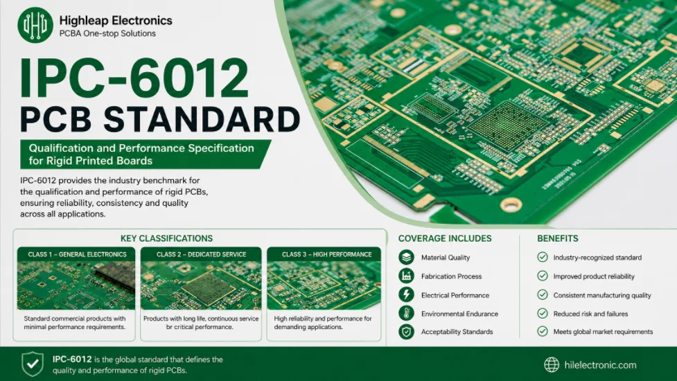
IPC-6012 Standard for Rigid PCB Fabrication
Figure 1. IPC-6012 standard for rigid PCB fabrication...

Electrical Testing PCB Flying Probe vs ICT vs FCT
Figure 1. Comparison of Electrical Testing PCB methods:...

Optimizing PCB Manufacturing and Assembly with Boundary Scan Technology
Introduction to Boundary-Scan Technology Boundary-scan,...

AOI for PCB and PCBA Inspection in Manufacturing
In the rapidly evolving electronics manufacturing...
How to get a quote for PCBs
Let us run DFM/DFA analysis for you and get back to you with a report.
You can upload your files securely through our website.
We require the following information in order to give you a quote:
-
- Gerber, ODB++, or .pcb, spec.
- BOM list if you require assembly
- Quantity
- Turn time
In addition to PCB manufacturing, we offer a comprehensive range of electronic services, including PCB design, PCBA (Printed Circuit Board Assembly), and turnkey solutions. Whether you need help with prototyping, design verification, component sourcing, or mass production, we provide end-to-end support to ensure your project’s success. For PCBA services, please provide your BOM (Bill of Materials) and any specific assembly instructions. We also offer DFM/DFA analysis to optimize your designs for manufacturability and assembly, ensuring a smooth production process.