
Back to blog
What is the Meaning of Schematic Diagram?

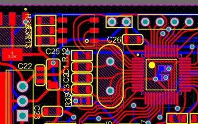
Partial schematic diagram of gas alarm
A schematic diagram is a fundamental aspect of PCB design, representing the functional connectivity between various electrical components. This guide aims to provide a comprehensive understanding of schematic diagrams, focusing on their importance, creation, interpretation, and best practices. This article is specially designed for PCB enthusiasts to improve your understanding of PCB design principles and ensure better implementation of your projects.
Understanding Schematic Diagrams
What is a Schematic Diagram?
A schematic diagram is a graphical representation of an electrical circuit. It uses standardized symbols to depict different components and lines to illustrate the connections between them. Unlike physical layouts, schematic diagrams focus on the logical relationships and flow of the circuit, making it easier to understand and troubleshoot.
Importance of Schematic Diagrams
Schematic diagrams are crucial for several reasons:
- Clarity: They provide a clear and organized view of the circuit, simplifying complex designs.
- Communication: They serve as a common language between engineers, designers, and technicians.
- Documentation: They document the design, facilitating maintenance and future upgrades.
- Debugging: They help identify and resolve issues by highlighting the connections and flow of the circuit.

Partial schematic diagram of gas alarm
Standards for Schematic Symbols
Schematic symbols are standardized globally to ensure consistency and understanding across different regions and industries. The primary standards are:
IEC 60617:The International Electrotechnical Commission (IEC) 60617 standard provides a comprehensive set of symbols for electrical and electronic components. It includes over 1750 symbols, ensuring detailed and accurate representation.
ANSI Y32:The American National Standards Institute (ANSI) Y32 standard, initially used for aircraft applications, has been adapted for general use. It aligns closely with IEC standards, ensuring global compatibility.
Common Schematic Symbols
Understanding common schematic symbols is essential for reading and creating diagrams. Here are a few examples:
-
- Resistors: Represented by a zigzag line or a rectangle.
- Capacitors: Depicted as parallel lines (for non-polarized) or a line and a curve (for polarized).
- Inductors: Shown as a series of loops or a rectangle with lines.
- Diodes: Represented by a triangle pointing to a line.
- Transistors: Depicted with arrows indicating the flow of current.
- Integrated Circuits (ICs): Shown as rectangles with multiple pins.

Common Schematic Symbols
Creating a Schematic Diagram
Creating a schematic diagram involves several steps, each requiring attention to detail and a clear understanding of the circuit. Here’s a step-by-step guide:
1. Define the Circuit Requirements
Before starting the schematic, outline the circuit’s functionality, components, and specifications. This ensures that the diagram will meet the design objectives.
2. Choose the Right Tools
Use advanced PCB design software, such as Altium Designer, Eagle, or KiCad, to create your schematic diagrams. These tools provide extensive libraries of symbols and automated features to simplify the process.
3. Generate Symbols
Create symbols for each component, ensuring they conform to the standard conventions. Include essential attributes like pin numbers, reference designators, and values.
4. Place Components
Arrange the symbols logically, grouping related components together. Place inputs on the left and outputs on the right to maintain a clear signal flow.
5. Draw Connections
Use lines to connect the components, representing the electrical connections. Ensure that lines intersecting at a junction have a node, indicating a connection.
6. Add Attributes
Include attributes for each component, such as resistance values for resistors, capacitance for capacitors, and voltage ratings for ICs. This information is crucial for selecting the right components during manufacturing.
7. Verify the Diagram
Double-check the schematic for errors, ensuring all connections are correct and all components are properly labeled. Use simulation tools to validate the circuit’s functionality.

Partial schematic diagram of oximeter
Best Practices for Drawing Schematic Diagrams
Adhering to best practices in schematic diagram creation is vital for ensuring clarity, accuracy, and ease of interpretation. Use standardized symbols in accordance with IEC or ANSI standards to maintain consistency and avoid confusion. Each component should be clearly labeled with reference designators and values to facilitate identification. Organize components logically, grouping related parts and maintaining a coherent signal flow to enhance readability. Minimize line crossovers to avoid misinterpretations and include comprehensive documentation with attributes and notes for each component. Regular reviews and updates of the schematic ensure it reflects any design changes and remains accurate.
Incorporating advanced techniques, such as differential pair routing and impedance control, is essential for high-frequency designs to reduce signal integrity issues. Utilize hierarchical schematics to manage complex designs by breaking them into functional blocks, simplifying the overall structure. Employ netlist generation to verify connections, ensuring the PCB layout accurately matches the schematic. Simulation tools are invaluable for validating the circuit’s performance before physical prototyping, identifying potential issues, and optimizing the design for better efficiency and reliability.
Reading and Interpreting Schematic Diagrams
To effectively read and interpret schematic diagrams, follow these steps:
1. Identify the Components
Start by identifying the components and their symbols. Familiarize yourself with the reference designators and attributes.
2. Understand the Connections
Trace the lines connecting the components, understanding how signals flow through the circuit. Look for nodes indicating connections and pay attention to the orientation of polarized components.
3. Analyze the Functionality
Consider the circuit’s purpose and how the components work together to achieve it. Use the attributes to understand the operational parameters and requirements.
4. Check for Anomalies
Look for any discrepancies or potential issues, such as missing connections, incorrect values, or conflicting attributes. Verify the schematic against the design requirements and specifications.
Advanced Topics in Schematic Diagrams
Hierarchical Schematics
For complex designs, use hierarchical schematics to break down the circuit into manageable sections. Each section represents a functional block, simplifying the design and debugging process.
Netlist Generation
A netlist is a data structure listing all the connections in a design. Generating a netlist from the schematic ensures that the PCB layout accurately reflects the design intent.
Simulation and Analysis
Use simulation tools to analyze the circuit’s performance before moving to the physical layout. Simulations help identify potential issues and optimize the design for better performance.
Conclusion
By understanding the standards, symbols, and best practices, you can create clear, accurate, and effective diagrams that facilitate the design, manufacturing, and maintenance of electronic circuits. Highleap Electronic is dedicated to providing top-quality PCB assembly services, ensuring your designs are brought to life with precision and reliability.
For further assistance and expert PCB assembly services, contact Highleap Electronic today. Request a quote and experience the difference in quality and service.
FAQs about Schematic Diagrams
1. What is the primary difference between a schematic diagram and a wiring diagram?
A schematic diagram shows the functional connections between components using standardized symbols, while a wiring diagram depicts the physical layout and connections of the components in a circuit.
2. How do schematic symbols differ between IEC and ANSI standards?
IEC symbols are more universally recognized and used globally, while ANSI symbols were initially developed for aircraft applications in the United States but have since been aligned with IEC standards.
3. Why is it important to include attributes like resistance, capacitance, and voltage in schematic diagrams?
Including these attributes ensures that the correct components are selected during manufacturing, and helps in understanding the operational parameters of the circuit.
4. How can hierarchical schematics simplify complex circuit designs?
Hierarchical schematics break down complex designs into functional blocks, making it easier to manage, understand, and troubleshoot each section of the circuit.
5. What role does simulation play in the schematic design process?
Simulation allows designers to test and analyze the circuit’s performance virtually, identifying potential issues and optimizing the design before moving to the physical layout stage.

Related Articles
Analysis of Power Supply Noise in HF PCB Design Process
This comprehensive guide explores the complexities of power supply noise, its origins, and advanced techniques to mitigate its effects in high-frequency PCB designs.
What is EMI, EMS and EMC?
At Highleap Electronic, we specialize in producing high-quality PCBs by integrating advanced techniques for impedance control, ensuring robust EMC and mitigating EMI.
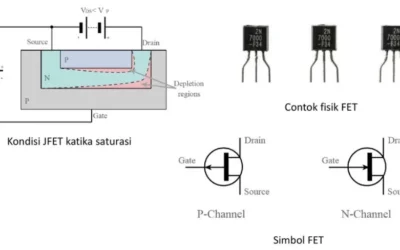
Understanding Field-Effect Transistors (FETs) in PCB Design
Dive into the fundamentals of Field-Effect Transistors (FETs) and their critical role in PCB design.
Take a Quick Quote