
Back to blog
Enhance Your PCBA Project:Comprehensive Guide to DIP Package

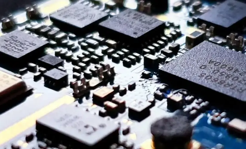
DIP PCB design drawing
In the rapidly evolving world of electronics manufacturing, understanding the impact and evolution of component packaging technologies such as the Dual In-Line Package (DIP) is crucial for any PCBA project. Originally introduced by Fairchild Semiconductor in 1964, the DIP was a revolutionary step toward standardizing the packaging of integrated circuits (ICs). This guide explores the DIP technology extensively, examining its inception, development, current applications, and future in the electronics industry, with a special focus on its role and adaptation in PCBA.
Historical Context and Development of DIP Technology
The adoption of DIP in the electronics industry marked a significant shift from using varied and proprietary packaging forms which hindered component interchangeability and large-scale production efficiencies. DIP technology allowed for a more standardized approach to IC packaging, significantly enhancing the manufacturability and reliability of electronic devices.
Key Developments:
- 1964: Introduction of the first 14-pin DIP by Fairchild Semiconductor.
- 1970s-1980s: Rapid adoption in consumer electronics, computing, and military applications.
- 1990s-Present: Gradual replacement by Surface Mount Technology (SMT) components, though DIP remains prevalent in specific applications due to its reliability and ease of use in prototyping and testing.
Power board DIP automatic equipment vertical material to horizontal material slow motion detailed real shot
Technical Deep Dive: DIP Configuration and Variants
DIP packages are characterized by their dual in-line configuration of pins which facilitate easy insertion into socketed or through-hole setups on PCBs. This section covers the various types of DIP packages, focusing on their materials, configurations, and suitability for different electronic components and applications.
DIP Package Types:
- Plastic DIP (PDIP): Commonly used for consumer electronics due to its cost-effectiveness and good electrical insulation properties.
- Ceramic DIP (CerDIP): Preferred in high-reliability applications such as aerospace and military due to its superior thermal and environmental resistance.
- Shrink DIP (SDIP): Offers a smaller footprint, enabling higher density on PCBs, suitable for compact devices.
- Metal DIP: While less common, metal DIPs offer enhanced thermal conductivity and EMI shielding, making them ideal for high-performance environments.

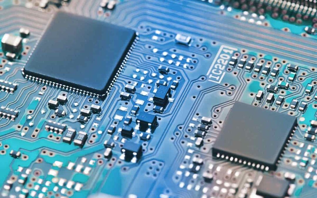
DIP components
Application and Implementation in PCBA
The practical application of DIP technology in PCBA involves various techniques and considerations to optimize the assembly process and ensure reliability and efficiency.
Key Processes:
- DIP Soldering and Post-Soldering: Techniques for securing DIP pins on a PCB, including wave soldering and manual soldering methods.
- Testing and Quality Assurance: Strategies to test and ensure the quality of DIP assemblies, including in-circuit testing and automated optical inspection.
- Design Considerations: Tips for incorporating DIP components in PCB design, focusing on layout, thermal management, and reliability.

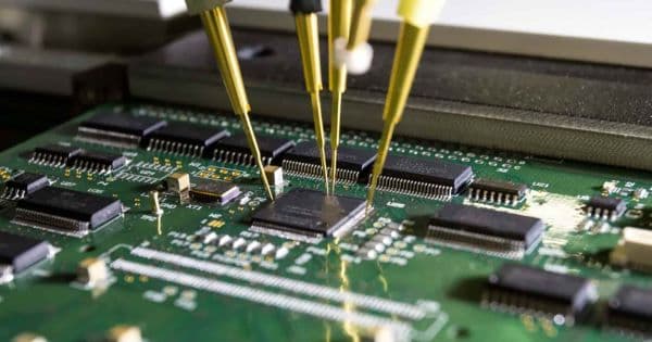
THT-DIP PCB
Challenges and Innovations
Despite its longevity, DIP faces challenges such as its larger physical size and manual assembly requirements, which can impact production scalability and cost. This section discusses how innovations in automated DIP assembly techniques and new materials are addressing these challenges.
Future Outlook:
- Automation in DIP Assembly: The development of more sophisticated DIP insertion machines and techniques that reduce labor costs and improve efficiency.
- Hybrid Techniques: Combining SMT and DIP technologies on the same PCB to leverage the advantages of both types of components.
- Advanced Materials: Research into new materials for DIP casings that enhance performance while reducing environmental impact.
The PCB vertical plug-in equipment in the video is an efficient circuit board plug-in equipment. It has the advantages of fast plug-in speed, high precision, suitable for various sizes and types of circuit boards.
Why will DIP equipment not be eliminated in 2024?
Although SMT (Surface Mount Technology) offers many manufacturing and design advantages such as faster production speeds and higher component density, DIP (Dual Inline Package) devices have not been phased out to date, Many netizens are puzzled as to why, even in 2024, devices from 30 years ago have not been phased out, and why our company is still using them. This is because Highleap Electronic is a PCB & PCBA manufacturer committed to customer satisfaction and quality assurance. We strive to meet popular demand and here are the reasons why we continue to use PCB Vertical Plugin equipment:
Convenience in prototyping and testing: DIP components are very convenient during the prototyping and testing stages due to their through-hole mounting characteristics. Engineers and designers can easily plug and unplug these components, which is extremely useful for making quick changes and debugging. This kind of flexibility is difficult to provide with SMT equipment.
Durability and mechanical stability: DIP-encapsulated components are generally stronger and more durable than SMT components. Since its pins pass through the PCB and are soldered to the other side, this provides better mechanical stability, especially in applications that need to withstand vibration or mechanical stress.
Compatibility and Availability: Many existing electronic devices and legacy projects are still designed to use DIP components because they are compatible and easy to replace and maintain. Furthermore, in the field of educational and hobby electronics, DIP components remain very popular due to their ease of handling and laboratory testing.
Cost-effectiveness: For some low-volume or specific applications, using DIP components may be more cost-effective. Although SMT equipment offers the advantages of automated production, the initial cost of equipment and setup can be higher. For those cost-sensitive projects, DIP provides an economically viable solution.
Application-specific needs: In some applications with high reliability requirements, such as the military and aerospace fields, DIP packaging may still be the first choice due to its excellent thermal performance and environmental tolerance. In addition, some special applications may require a specific type of DIP package, such as a ceramic DIP package, which provides higher thermal stability and environmental protection.
In conclusion, despite the dominance of SMT technology in modern electronics manufacturing, DIP technology still maintains its importance due to its advantages in design flexibility, durability, cost-effectiveness and specific applications. Both technologies have their own merits and are usually chosen based on the needs and conditions of a specific project.
Conclusion
DIP technology has played a foundational role in the electronics industry. Its evolution from a groundbreaking innovation to a standard component of PCBA exemplifies the dynamic nature of technology adoption and adaptation in electronics manufacturing. As we look towards the future, DIP technology continues to adapt, ensuring its place in the industry through continuous improvement and innovation.
This guide not only serves as a historical account but also as a technical and practical reference for electronics manufacturers, engineers, and designers. Highleap Electronic, with its extensive experience and technical expertise, remains at the forefront of delivering high-quality PCBA solutions incorporating advanced DIP technologies.
FQA
1.What makes DIP technology particularly suited for educational and hobby electronics?
DIP components are favored in educational and hobbyist settings because of their user-friendly nature. Their through-hole design simplifies the process of manually inserting and removing components on PCBs, which is ideal for learning environments and DIY projects where adjustments and hands-on experience are crucial.
2.How does the physical size of DIP components affect their use in modern electronics?
The larger physical size of DIP components compared to SMT components can be a drawback in compact and densely packed electronic devices. However, this size can be advantageous in applications requiring robust mechanical stability and ease of handling, such as in prototyping or in environments prone to mechanical stress.
3.Can DIP and SMT components be used together on the same PCB? If so, what are the benefits?
Yes, DIP and SMT components can be integrated on the same PCB to combine the strengths of both technologies. This hybrid approach allows for the high density and automated production advantages of SMT while retaining the mechanical robustness and ease of prototyping provided by DIP components.
4.What are the environmental impacts of using DIP components, and how are new materials addressing these concerns?
Traditional DIP components can pose environmental challenges due to the materials used in their construction. However, recent advances include the development of new, eco-friendly materials for DIP casings that reduce environmental impact without compromising performance.
5.What future developments are anticipated in DIP technology to keep it relevant in the electronics manufacturing industry?
The future of DIP technology involves enhancing automation in the assembly process to reduce labor costs and improve production efficiencies. Innovations in material science are also expected to produce DIP components that offer better performance and environmental sustainability. Additionally, combining DIP with modern SMT techniques on PCBs can optimize the advantages of both technologies in future applications.
PCB & PCBA quick quote
Related Articles
What is the difference between SMD and SMT?
PCB SMTSurface Mount Technology (SMT) and Surface Mount Devices (SMD) are crucial concepts in the field of electronics manufacturing, specifically in the assembly of printed circuit boards (PCBs). Both terms are integral to the modern methods of producing electronic...
Flexible PCB Cost Optimization Strategy
flexible PCBIn the realm of contemporary electronics, the proliferation of flexible PCBs stands as a testament to the industry's evolution toward miniaturization and functionality. Unlike the more traditional rigid PCBs, which benefit from simpler production...
High Volume Turnkey PCB Assembly Services
PCB assembly servicesPrinted Circuit Board Assembly (PCBA) is a critical process in electronics manufacturing, where various electronic components are soldered onto a PCB to create a functional electronic device. This comprehensive guide explores the PCB assembly...
Reliable PCBs: The Role of Functional Circuit Testing
Functional Circuit TestingIn the realm of PCB manufacturing, ensuring the functionality and reliability of the boards is paramount. Functional Circuit Test (FCT) is a crucial step in this process, serving as the final check before the boards are released into the...
Take a Quick Quote