
Back to blog
How to Choose the Right Smart Home PCB – PCB Manufacturing

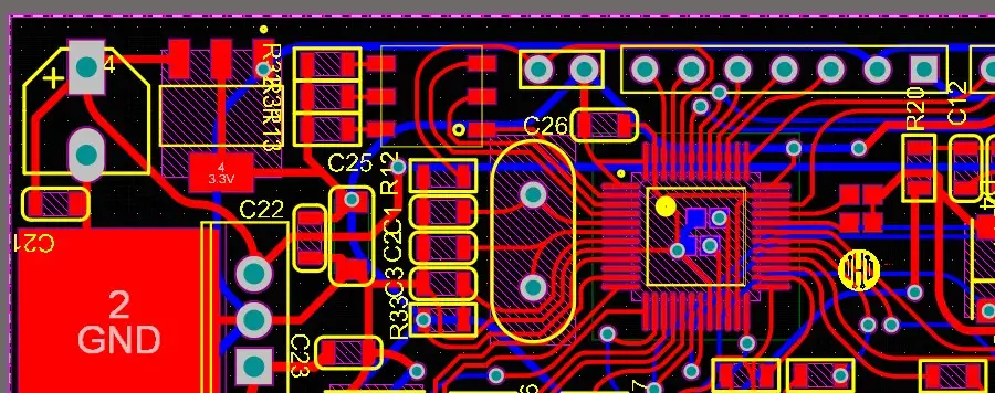
Smart Home PCBA
The concept of a “smart home” has evolved significantly in the digital age, primarily due to advancements in Internet of Things (IoT) technology and smart devices. The Smart Home PCB represents a vital element in the design, manufacturing, and functioning of smart home devices. These PCBs are specifically engineered to ensure the seamless connectivity, automation, and performance of interconnected appliances like lighting, heating systems, security devices, and more. In this extensive article, we delve into the technicalities, challenges, and future of smart home PCB design, highlighting its critical role in emerging technologies.
The Importance of Smart Home PCB Design in Emerging Technology
Smart home PCB design forms the foundation for creating innovative, reliable, and energy-efficient smart devices. The PCB acts as the central hub for communication and data exchange between various components within a smart system, from security cameras to lighting systems. The intricacies involved in PCB design, including prototyping and layout engineering, directly influence the device’s performance and reliability. As homes increasingly rely on intelligent technologies, the PCB’s role in enabling robust connectivity and seamless operation becomes ever more crucial.
Key Considerations in Smart Home PCB Design
Designing PCBs for smart home applications requires careful consideration of several factors to ensure optimal device performance:
- Device Analysis and Requirements: Understanding the intended use of the device informs the selection of sensors, electronic components, and communication modules. A thorough analysis ensures the PCB design aligns with the device’s purpose and functionality.
- Prototyping and Conceptualization: Conceptualizing the PCB’s features and functions involves creating a prototype to validate and test the design. Choosing the right components is crucial for the PCB’s reliability and functionality.
- Schematic Design and PCB Layout: The schematic diagram outlines the electrical connections and component structure on the PCB, serving as a blueprint for the actual layout. Specialized software tools like Altium or Eagle help design the real-time layout for fabrication.
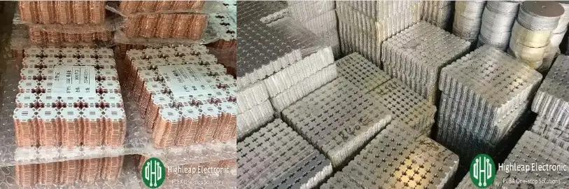
- Fabrication, Assembly, and Manufacturing: The fabrication process involves preparing panels, circuit imaging, and plating copper layers. The assembly involves etching, soldering components, and mounting them onto the PCB, typically using automated pick-and-place machines.
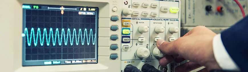
- PCB Testing and Inspection: Rigorous electrical testing and inspection ensure the PCB adheres to design specifications and functions correctly.
- Finalization and Programming: Firmware programming ensures the PCB functions correctly and communicates effectively with the user and other devices.

Application of smart home PCBA
Challenges in Smart Home PCB Design
1.Miniaturization
The trend towards compact smart devices means that designers must develop PCBs with significantly smaller components and a reduced physical footprint. This miniaturization poses substantial challenges in component placement, routing, and maintaining signal integrity. As devices become smaller, designers are tasked with balancing the need for compactness without compromising performance or reliability. High-density interconnect (HDI) techniques and advanced multilayer PCB designs are often required to pack more functionality into smaller spaces. This complexity necessitates meticulous planning and careful consideration of heat dissipation, signal paths, and potential interference.
2.Power Efficiency
In smart home applications, power efficiency is crucial due to the continuous operation of devices and the growing emphasis on sustainability. Designers need to optimize power distribution to ensure low energy consumption while maintaining device performance. This involves carefully selecting power-efficient components and designing power distribution networks that minimize voltage drops and power loss. Poorly designed PCBs can result in excessive heat generation, high power consumption, and reduced device reliability. Advanced power management strategies, such as low-power design techniques and dynamic power scaling, can help mitigate these issues.
3.Signal Integrity and EMI
Signal integrity issues and electromagnetic interference (EMI) are significant concerns in the design of smart home PCBs. Signal integrity refers to the quality and reliability of the electrical signals traveling through the PCB. Factors like signal reflection, crosstalk, and noise can severely degrade signal quality, leading to data loss or device malfunction. Similarly, EMI can disrupt the operation of sensitive components and systems, particularly in environments with multiple interconnected devices. To address these challenges, designers must use controlled impedance traces, proper grounding techniques, and shielding strategies to ensure signal fidelity. Adhering to design guidelines and standards for signal routing, grounding, and component placement is essential in mitigating these issues.
Addressing these challenges requires a combination of design expertise, advanced software tools, and a thorough understanding of the operating environment to develop reliable and efficient PCBs for smart home devices.
The Future Development of Smart Home PCB Design
Smart home PCB technology is rapidly evolving, driven by key trends like miniaturization and AI integration. The demand for smaller, more efficient devices pushes designers towards innovative sensor integration and advanced user interfaces. AI and machine learning integration into PCBs allows for intelligent decision-making, enhancing device response times and accuracy.
The future of smart home PCBs is defined by the need for seamless wireless connectivity, energy efficiency, and reliable communication between devices. The push for compact, IoT-enabled devices will significantly influence PCB design, necessitating advanced techniques to meet growing demands.
Why choose Highleap Electronic when making Smart home PCB?
hoosing Highleap Electronic to manufacture smart home PCBs offers several strategic advantages, especially for customers who are committed to developing high-quality, reliable and innovative smart home devices. Here are the key reasons why Haiyue Electronics stands out in the PCB manufacturing industry:
Advanced manufacturing capabilities:
Highleap Electronic is equipped with state-of-the-art manufacturing facilities that can handle complex PCB designs and requirements. They employ modern technologies such as high-density interconnect (HDI) manufacturing, which is critical for miniaturization without compromising the performance of smart home devices. This feature is critical for integrating multiple functions onto a single board with high reliability.
Comprehensive quality assurance:
Haiyue Electronics attaches great importance to quality assurance at every stage of the PCB manufacturing process. From rigorous raw material inspection to sophisticated in-process quality control measures and final testing, Highleap ensures every PCB meets the highest quality and reliability standards. Meticulous attention to quality helps reduce the incidence of failures and extends the life of your equipment.
Cutting-edge design supports:
Highleap Electronic offers a wide range of design support services to its customers. This includes assistance with PCB layout design, schematic review and simulation services to ensure optimal performance. Their expertise in signal integrity, power management and EMI reduction can greatly benefit smart home device manufacturers, especially when dealing with complex designs and new technologies.
Flexible production scale:
Whether you require prototypes or large-scale production, Highleap Electronic can meet different needs without compromising turnaround time or quality. Their flexible production capabilities make them an ideal partner for startups and established companies looking to innovate quickly and efficiently.
Environmental Compliance:
Highleap Electronic adheres to strict environmental regulations and ensures that all PCBs are manufactured using environmentally friendly processes and materials. This commitment not only helps reduce environmental impact, but also aligns with the sustainability goals of many companies developing smart home devices.
Customer-centric approach:
Highleap Electronic is known for its customer-centric approach, providing personalized service and support throughout the manufacturing process. They work closely with customers to understand their specific needs and challenges, providing tailored solutions that meet the unique requirements of smart home technology.
Global supply chain and logistics:
With a strong global supply chain and efficient logistics capabilities, Highly Electronics ensures timely delivery of PCBs to anywhere in the world. The reliability of supply chain management is critical for companies that want to maintain stable production schedules and market launches.
By partnering with Haiyue Electronics, smart home device manufacturers can leverage advanced PCB technology and comprehensive support to develop products that are not only technologically advanced but also perform reliably and efficiently. This makes Haiyue Electronics a compelling choice in the highly competitive field of smart home PCB manufacturing.
Conclusion
Smart home PCB design and manufacturing require meticulous attention to emerging challenges and technological advancements. The industry is evolving towards more compact designs, energy-efficient systems, and seamless connectivity. Integrating AI and machine learning directly into PCBs will not only enhance device intelligence but also improve performance and minimize dependencies. A holistic approach that balances technological advancement, user experience, and sustainability will drive the success of smart home PCB design in the future.
FQA
1. What specific technologies are commonly used to achieve miniaturization in smart home PCBs?
Answer: To achieve miniaturization in smart home PCBs, technologies such as High-Density Interconnect (HDI), microvias, and multi-layer PCBs are commonly used. These techniques allow for more compact designs by reducing the physical footprint of the components while maintaining high levels of functionality and performance.
2. How does smart home PCB design impact power efficiency in smart devices?
Answer: Smart home PCB design plays a crucial role in power efficiency by optimizing power distribution networks and using low-power components. Proper design can help reduce voltage drops and minimize power loss, ensuring that smart devices consume less energy and remain operational for longer periods.
3. What are the primary methods used to improve signal integrity in smart home PCBs?
Answer: Improving signal integrity in smart home PCBs involves using controlled impedance traces, proper grounding, and shielding techniques. Additionally, maintaining appropriate spacing between traces and using differential pair routing can help reduce signal degradation and ensure reliable data transmission.
4. How does the integration of artificial intelligence (AI) affect smart home PCB design?
Answer: Integrating AI in smart home PCBs introduces additional requirements for processing power and data handling. Designers must incorporate specialized components such as AI chips and ensure that the PCB can support the increased computational workload without compromising signal integrity or power efficiency.
5. What considerations are important for ensuring robust wireless connectivity in smart home PCBs?
Answer: Ensuring robust wireless connectivity in smart home PCBs requires careful antenna design, strategic placement of wireless modules, and minimizing interference from other components. It is crucial to optimize the PCB layout to prevent signal degradation and maintain strong and stable wireless connections across various smart devices.
PCB & PCBA quick quote
Related Articles
Analysis of Power Supply Noise in HF PCB Design Process
Power Supply PCB Design Partial FilesIn the realm of high-frequency PCB design, effective management of power supply noise is crucial to maintaining optimal system performance. As electronic devices evolve with higher clock speeds and increased component density, the...
What is EMI, EMS and EMC?
EMC TestElectromagnetic compatibility (EMC) is a critical consideration in the design and manufacturing of electronic devices, especially on PCBs. This article aims to delve into the concepts of Electromagnetic Interference (EMI), Electromagnetic Susceptibility (EMS),...

Boosting PCB Manufacturing Efficiency with Laser Direct Imaging (LDI)
PCB produced by LDI exposureUnderstanding Laser Direct Imaging Technology Fundamental Principles of LDI Laser Direct Imaging (LDI) revolutionizes traditional photolithography by utilizing precisely controlled laser beams in place of UV light and physical masks. This...
Types of LED PCB Boards and Their Industry Applications
LED PCB BoardsLED PCB boards, known for their efficiency and versatility, play a crucial role in modern lighting solutions. This article delves into the intricacies of LED PCB boards, including their construction, types, applications, and benefits. We will also...
Take a Quick Quote