
Application of High Density Interconnect PCB in High-Tech

What is HDI PCB?
HDI PCBs (High-Density Interconnect PCBs) are a type of printed circuit board that offer higher wiring density per unit area compared to traditional circuit boards. They are designed to meet the demands of smaller and faster electronic products.
HDI technology allows for a more compact design by incorporating smaller vias, pads, copper traces, and spaces on the PCB. This enables denser routing, resulting in a PCB that is lighter, more compact, and requires fewer layers. With HDI, a single board can accommodate the functionalities that would typically require multiple boards in a device.
HDI PCBs are particularly useful for high-layer and expensive laminated boards, as they offer increased functionality in a smaller form factor. They are commonly used in applications where space is limited but the need for high-performance electronics is critical, such as smartphones, tablets, and other portable devices.
Overall, HDI PCBs contribute to the miniaturization and improved performance of electronic devices by providing a higher level of integration and improved signal integrity.
What Makes HDI PCBs Unique?
High-Density Interconnect (HDI) PCBs are unique in several ways compared to traditional PCBs. Their advanced technology offers higher circuitry density per unit area, which allows for more functionality and miniaturization. Here’s what sets HDI PCBs apart:
- Smaller Components: HDI PCBs can accommodate smaller components and shorter interconnections, leading to faster signal transmission and a reduction in signal loss.
- Multiple Layers: These boards often come with multiple layers stacked together, interconnected through vias, which can be blind vias (connecting an outer layer to an inner layer), buried vias (connecting two inner layers but not visible from the outer layers), or through vias (going through the entire board).
- Improved Signal Integrity: Due to shorter paths and smaller components, HDI PCBs typically offer better signal integrity, reducing both the inductance and capacitance of the circuit.
- High Frequency and Speed: The reduced size and enhanced capabilities allow these boards to operate at higher frequencies and speeds, making them ideal for modern, high-speed, complex circuitry.
- Increased Interconnection Density: HDI technology enables a larger number of connections to fit into a smaller area, which is particularly useful for complex devices like smartphones, tablets, and medical equipment.
- Reduced Size and Weight: Because of the high circuitry density, HDI PCBs can be much smaller and lighter than traditional PCBs, making them suitable for portable and miniaturized devices.
- Improved Thermal Management: The design of HDI PCBs allows for better thermal management techniques, which can be crucial for high-performance computing and automotive applications.
- Cost Factor: While the technology offers many advantages, it is generally more expensive to produce than traditional PCBs due to the specialized processes and materials involved.
- Design Complexity: Designing an HDI PCB often requires specialized software and expertise due to the complexity of the layout, the multiple layers, and the smaller components.
- Advanced Materials: HDI PCBs often utilize advanced materials like high-frequency laminates to meet specific performance criteria.
These unique characteristics make HDI PCBs increasingly popular in modern electronics where space, weight, and higher performance capabilities are critical factors.
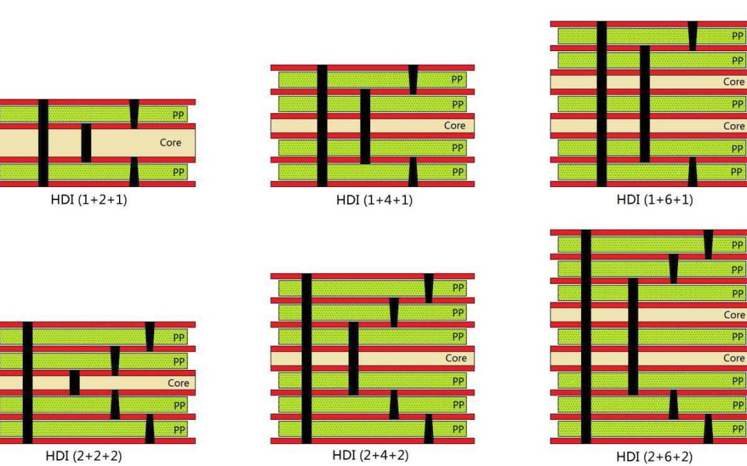
Types of Vias in HDI PCBs

In High-Density Interconnect (HDI) Printed Circuit Boards (PCBs), vias play a crucial role in providing electrical connections between the layers of the board. The types of vias used in HDI PCBs are more advanced than those in standard PCBs, and they enable higher component density and improved performance. Here are the main types of vias used in HDI PCBs:
- Through Vias: These are the simplest type and go all the way through the PCB from the top layer to the bottom layer. While they are commonly used in traditional PCBs, they are less frequently used in HDI boards due to their size and the space they occupy.
- Blind Vias: These vias connect an outer layer to one or more inner layers but do not go all the way through the board. This allows for more efficient use of board real estate, enabling higher component density.
- Buried Vias: These are hidden within the board and connect two or more inner layers but are not accessible from the outer layers. Like blind vias, buried vias also save space on the outer layers for components.
- Microvias: These are very small vias with a diameter usually less than 150 micrometers. They are generally used to connect only adjacent layers, whether from an outer layer to the first inner layer (as a blind microvia) or between two inner layers (as a buried microvia). Due to their small size, they enable much higher component density and are often used in the latest HDI technologies.
- Stacked Vias: These are vias that are directly on top of each other and are used to connect multiple layers. Stacked vias can be a combination of microvias, blind vias, or through vias.
- Staggered Vias: Unlike stacked vias, staggered vias are offset from each other. This arrangement allows for connections between multiple layers without the vias being directly on top of each other.
- Filled Vias: Sometimes, vias are filled with a conductive or non-conductive material to either provide structural integrity or to prepare the surface for a flat component to be placed on top.
- Via-in-Pad: This is a design technique where a via is placed directly beneath a component pad. This allows for a direct interconnection between the surface layer and the inner layers without the need for additional traces, thus saving space.
Each type of via has its own advantages and limitations, and the choice of which to use depends on the specific requirements of the electronic device being designed. Issues such as signal integrity, component density, thermal management, and cost all play a role in determining the most suitable type of via for a given HDI PCB application.
HDI PCB Design Guide
Stack-Up and Microvia Structure
Begin by planning your stack-up, deciding on the number of layers and their arrangement. Choose the appropriate microvia types—blind, buried, or through-hole—based on your design requirements. This initial step is crucial to ensure your design meets the necessary specifications and performance criteria.
Material Selection and Signal Integrity
Opt for high Tg (glass transition temperature) materials to achieve better thermal stability, and select materials with a low Coefficient of Thermal Expansion (CTE) to minimize expansion issues. Ensure that trace widths are optimized for the signals you are routing, and use impedance calculators to match the impedance of traces and components, maintaining signal integrity and controlled impedance throughout the design.
Routing, Placement, and Thermal Management
Place components strategically to minimize the length of critical signal paths and use the shortest, most direct routes for critical signals. For thermal management, incorporate heat sinks for high-heat components and utilize thermal vias to dissipate heat away from hot areas. Proper routing and placement are essential to maintaining signal integrity and managing heat effectively.
DFM, Testing, and Validation
Ensure manufacturability by maintaining adequate annular ring sizes for vias and proper trace spacing to avoid shorts. Generate and thoroughly check Gerber files, and always create a prototype before mass production. Consider material compatibility to avoid CTE mismatch, limit the number of lamination cycles to control costs and signal integrity, and consult with your PCB manufacturer for design validation. Perform multiple quality checks to ensure the board meets all design criteria, focusing on thermal aspects for high-speed or high-power designs.
Applications of HDI PCB
High-Density Interconnect (HDI) Printed Circuit Boards (PCBs) are widely used in various industries due to their ability to support more components in a smaller space, offer better electrical performance, and enhance reliability. Here are some of the key applications of HDI PCBs:
Consumer Electronics
Smartphones
- Miniaturization: HDI PCBs allow for a smaller form factor, enabling sleek and slim smartphone designs.
- Multi-layering: Multiple layers can be stacked for integrating more components, such as processors, memory, and sensors.
- Signal Integrity: HDI PCBs offer better signal integrity, crucial for high-speed data processing and communications in smartphones.
Laptops and Tablets
- Thermal Management: HDI PCBs are effective in dissipating heat, which is vital for high-performance laptops.
- High-speed Data Transfer: USB-C and Thunderbolt ports benefit from the high-speed capabilities of HDI PCBs.
Automotive Industry
Advanced Driver Assistance Systems (ADAS)
- Radar Systems: HDI PCBs are used in compact radar modules for better resolution and range.
- Camera Systems: The small size of HDI PCBs allows for discreet integration of cameras in vehicles.
Electric Vehicles (EVs)
- Battery Management Systems (BMS): HDI PCBs are used in BMS for better efficiency and safety.
- Charging Units: Fast-charging technology relies on HDI PCBs for efficient power conversion and management.
Medical Devices
Portable Equipment
- Ultrasound Machines: HDI PCBs enable the miniaturization of ultrasound devices without compromising on performance.
- MRI Machines: They are used in the signal processing units of portable MRI machines.
Wearable Monitors
- Heart Rate Monitors: HDI PCBs are used for their low power consumption and small form factor.
- Glucose Monitors: The compact design of HDI PCBs allows for non-intrusive wearable devices.
Aerospace and Defense
Radar Systems
- Signal Integrity: HDI PCBs offer better signal integrity, crucial for radar accuracy.
- Durability: They are designed to withstand extreme environmental conditions.
Communication Equipment
- Satellite Radios: HDI PCBs are used in satellite radios for better frequency response and reliability.
- Navigation Systems: GPS and other navigation systems benefit from the high-speed capabilities of HDI PCBs.
Industrial Automation
Control Systems
- Programmable Logic Controllers (PLCs): HDI PCBs are used in PLCs for better performance and reliability.
- Human-Machine Interface (HMI): Touch panels and displays use HDI PCBs for better responsiveness.
Sensors
- Temperature Sensors: HDI PCBs are used for their high sensitivity and accuracy.
- Pressure Sensors: They are used in pressure sensors for better calibration and measurement.
Telecommunications
Networking Equipment
- Routers and Switches: HDI PCBs are used for high-speed data transmission and low latency.
- Base Stations: Cellular base stations use HDI PCBs for better signal integrity and range.
IoT Devices
Smart Home Devices
- Smart Thermostats: HDI PCBs enable more accurate temperature control and scheduling features.
- Smart Locks: They are used in smart locks for better security features and connectivity.
Industrial IoT
- Sensors and Controllers: HDI PCBs are used in industrial sensors for better data collection and transmission.
- Gateways: Industrial IoT gateways use HDI PCBs for robust and reliable data transmission.
Computing and Data Storage
Servers
- Data Transmission: HDI PCBs are used in servers for high-speed data transmission.
- Cooling Systems: They are used in cooling systems for better thermal management.
Data Centers
- Networking Equipment: Switches, routers, and other networking devices in data centers use HDI PCBs for high-speed and reliable data transmission.
Test and Measurement
Oscilloscopes
- Signal Integrity: HDI PCBs are used in high-frequency oscilloscopes for better signal integrity and accuracy.
Signal Generators
- Frequency Range: HDI PCBs enable a wider frequency range in signal generators.
HDI PCBs are a preferred choice for high-layer and expensive laminated boards, and Highleap is a leading PCB and PCBA manufacturer that specializes in producing high-quality HDI PCBs. With their expertise in advanced PCB fabrication and assembly, Highleap provides comprehensive solutions for customers in various industries, including telecommunications, consumer electronics, medical devices, and more. Their commitment to quality, reliability, and customer satisfaction makes them a trusted partner for companies seeking high-density interconnect solutions. Whether it’s designing and prototyping HDI PCBs or delivering large-scale production, Highleap offers end-to-end services to meet the unique requirements of their clients.
Conclusion
High-Density Interconnect (HDI) PCBs are advanced printed circuit boards designed to accommodate higher wiring density per unit area, making them ideal for smaller and faster electronic products. HDI technology achieves a more compact design by using smaller vias, pads, copper traces, and spaces, resulting in lighter and more compact PCBs that require fewer layers. These characteristics make HDI PCBs particularly useful in applications where space is limited but high performance is essential, such as in smartphones, tablets, and other portable devices. They provide significant benefits, including improved signal integrity, higher component density, and better thermal management.
The unique features of HDI PCBs, such as the use of blind, buried, and microvias, allow for higher functionality and miniaturization, making them a crucial component in modern high-performance electronics. Furthermore, their advanced material requirements and complex design processes, including specialized software and expertise, distinguish them from traditional PCBs. HDI PCBs are increasingly popular in various industries, including consumer electronics, automotive, medical devices, aerospace, and telecommunications, where compact size, reduced weight, and enhanced performance are critical.
High Density Interconnect PCB FAQs
What Are the Key Benefits of Using High Density Interconnect PCBs Over Traditional PCBs?
High Density Interconnect PCBs offer enhanced performance in terms of signal integrity, higher component density, and better thermal management, making them ideal for modern, high-speed electronic devices.
How Do High Density Interconnect PCBs Improve Signal Integrity in High-Frequency Applications?
High Density Interconnect PCBs utilize shorter trace paths and smaller vias, which reduce signal loss and interference, thus providing better signal integrity for high-frequency applications.
What Factors Should Be Considered When Selecting Materials for High Density Interconnect PCBs?
When selecting materials for High Density Interconnect PCBs, consider the glass transition temperature (Tg), coefficient of thermal expansion (CTE), and compatibility with the specific application’s thermal and mechanical requirements.
How Does the Design Process for High Density Interconnect PCBs Differ from Standard PCBs?
The design process for High Density Interconnect PCBs involves more complex routing, smaller component placement, and the use of advanced via structures such as blind, buried, and microvias, requiring specialized design software and expertise.
What Are the Common Applications of High Density Interconnect PCBs in Modern Electronics?
High Density Interconnect PCBs are commonly used in consumer electronics (smartphones, tablets), automotive systems (ADAS, EVs), medical devices (portable and wearable equipment), aerospace, and telecommunications due to their compact size and high performance.

Recommended Posts

Comprehensive Guide to Plated Through-Hole (PTH) Technology in PCB Manufacturing
[pac_divi_table_of_contents title="On this article"...

Mastering Staggered and Stacked Vias: Advanced PCB Design Techniques for High-Performance Electronics
An important part of modern PCB design is PCB drilling -...

High Density Interconnect PCB Guide | Highleap Electronics
[pac_divi_table_of_contents...
HDI Layout Best Practices: Key Design Tips for HDI Circuit Boards
HDI stack diagram in HDI circuit board factoryIntroduction...
Discover how our expertise can help with your next PCB project.