
Back to blog
Veteran engineers share PCB design insights with 10+ years

PCB schematic diagram–PCB design insights
Introduction
With over a decade of experience as a seasoned PCB design engineer, I’ve witnessed firsthand the rapid evolution and increasing demands in this field. This comprehensive guide aims to impart critical insights and cutting-edge techniques that will elevate your PCB design skills to effectively meet the challenges of modern electronics.
Today’s PCBs are not merely interconnect platforms; they are integral components that profoundly influence the performance, reliability, and manufacturability of electronic devices. From high-speed digital circuits to sensitive analog designs, and from compact wearables to robust industrial equipment, effective PCB design principles are more crucial than ever. This extensive blog post delves deep into the intricate world of PCB design, covering everything from initial conceptualization to final production-ready layouts. We explore advanced techniques for managing signal integrity in high-speed designs, strategies for efficient power distribution, thermal management considerations, and much more.
Essential Steps for PCB Design Preparation
Effective PCB design begins with meticulous preparation, starting with the creation of a comprehensive component library. While software-built libraries offer convenience, they often lack specificity. Therefore, customizing the library based on standard component specifications ensures precise integration into the PCB layout. Prioritize the PCB component library, as it directly influences board installation. Meanwhile, the SCH component library, though less demanding, requires accurate pin definition for seamless connectivity.
Designing the Schematic Diagram
Once the component libraries are established, the next step is crafting the schematic diagram. This critical phase involves translating circuit design into a detailed schematic layout. Focus on clarity and accuracy to facilitate smooth transition to PCB layout.
PCB Layout Implementation
With the schematic finalized, proceed to PCB layout design. Build upon the schematic foundation, ensuring components are positioned optimally for functionality and manufacturability. Pay attention to detail, as this phase sets the stage for the board’s electrical and mechanical performance.
Advanced PCB Materials and Structures
PCB Structure Design
The initial phase of PCB development involves meticulous planning within the PCB design environment, focusing on precise adherence to circuit board dimensions and mechanical positioning criteria. Essential elements such as connectors, buttons/switches, screw holes, and assembly holes are strategically placed to meet exact specifications. Special attention is given to segregating routing and non-routing areas; for example, non-routing zones around screw holes prevent interference, ensuring optimal board functionality and reliability.
High-Frequency Materials
In applications demanding high-frequency performance, the selection of PCB materials is critical:
- Rogers RO4350B is preferred for its minimal dielectric loss (tanδ ≈ 0.0037 at 10 GHz).
- Taconic RF-35 offers stability across a broad temperature range.
- PTFE-based materials excel in applications requiring extremely low loss.
Hybrid and Mixed-Material Designs
Advanced PCB designs often integrate multiple materials to enhance functionality:
- Rigid-flex designs combine rigid FR-4 with flexible polyimide, ideal for applications needing both flexibility and rigidity.
- Mixed-dielectric stackups optimize signal integrity while balancing cost considerations.
Advanced PCB Structures
Innovative PCB structures go beyond conventional approaches:
- Embedded passives and actives increase integration density and performance efficiency.
- Cavity designs accommodate irregularly shaped components within the PCB layout.
- Vertical conductive structures (VeCS) facilitate high-density interconnects, enhancing overall PCB design flexibility and functionality.
Best Practices in PCB Layout and Component Placement
PCB layout involves strategically placing components on the board to optimize performance and manufacturability. Once preliminary preparations are complete, such as generating a netlist from the schematic and importing it into the PCB layout software, components are positioned on the board with wire connections indicated.
Key principles for effective layout include:
- Segmentation Based on Electrical Performance: Divide the board into distinct areas such as digital circuits (susceptible to interference), analog circuits, and power drive sections (potential sources of interference).
- Proximity and Connectivity: Place components of similar function close together to simplify connections. Adjust the relative positions of functional blocks for straightforward routing.
- Consideration of Component Characteristics: Position large and heavy components thoughtfully to ensure installation strength. Separate heat-generating components from temperature-sensitive ones, implementing heat dissipation measures if necessary.
- Strategic Component Placement: Place I/O driver components near board edges and output connectors for efficient signal management. Position clock generators (e.g., crystals or oscillators) in close proximity to components utilizing the clock signal.
- Decoupling and Additional Components: Incorporate decoupling capacitors (e.g., high-frequency ceramic capacitors) between the power input pin and ground for each integrated circuit. In dense layouts, consider adding tantalum capacitors around integrated circuits. Include snubber diodes (e.g., 1N4148) at relay coils to manage voltage spikes.
- Achieving Balance in Layout: Maintain a balanced layout with a structured arrangement that avoids being overly dense or sparse. Ensure components are uniformly oriented and neatly organized, enhancing both board appearance and ease of routing.
Careful consideration of component size, height, and relative positions during placement is crucial for optimizing electrical performance, feasibility of production, and installation convenience. This meticulous approach not only enhances functionality but also streamlines manufacturing processes.

PCB engineer inspects Gerber file diagram
Optimal Routing Strategies for High-Performance PCB Design
Routing is a critical phase in PCB design, directly impacting board performance. It encompasses three primary levels:
- Basic Routing: The fundamental requirement is completing all traces without any unconnected wires, ensuring the board meets minimum operational standards.
- Electrical Performance: This stage ensures the board’s functionality meets design specifications. Traces are meticulously adjusted post-basic routing to optimize electrical characteristics.
- Aesthetics: Beyond functionality, clean and organized routing enhances ease of testing and maintenance. Chaotic or messy routing, despite meeting electrical standards, can hinder board usability.
Key Routing Principles:
- Prioritize Power and Ground: Begin by routing power and ground traces to establish a robust electrical foundation. Ground traces should be as wide as feasible within design constraints, following the hierarchy: ground > power > signal. Digital circuits benefit from a dedicated ground plane to form a comprehensive ground network (analog circuits employ alternative methods).
- Handle High-Frequency Traces First: Route high-frequency traces with care, avoiding parallelism between input and output traces to mitigate reflection interference. Use ground traces for isolation where necessary, ensuring perpendicular routing on adjacent layers to minimize parasitic coupling.
- Clock and High-Speed Circuit Considerations: Ground the oscillator housing and keep clock traces short and direct. Maintain a clear area around these components, reducing the surrounding electric field. Avoid routing other signal traces above critical high-speed circuits.
- Routing Techniques: Prefer 45-degree angled routing over 90-degree angles to reduce high-frequency signal radiation; curved routing can also be beneficial for high-demand traces. Avoid creating signal trace loops; if unavoidable, minimize their size. Limit the number of vias for signal traces.
- Critical Signal Handling: Critical traces should be short and thick, flanked by ground traces for protection. Use the “ground-signal-ground” method for flat cable routing carrying sensitive or noise-carrying signals. Reserve test points for production and maintenance testing on critical signals.
- Optimization and DRC: After initial schematic routing, optimize the layout. Conduct a comprehensive network check and pass the Design Rule Check (DRC). Fill unrouted areas with a ground plane using substantial copper or employ multi-layer boards with dedicated power and ground layers for enhanced performance.
Implementing these routing strategies ensures not only electrical integrity but also facilitates efficient testing, maintenance, and overall reliability of high-performance PCB designs.
Perfecting Your PCB Design: The Art of Continuous Improvement
Design refinement is an ongoing pursuit in PCB development, guided by the principle of “there is no best, only better.” Despite the meticulous crafting of initial designs, there always exists room for enhancement. Experience indicates that optimizing a design typically requires twice the effort invested in its initial routing phase. Once potential modifications are thoroughly addressed, the process of copper filling, crucial for grounding and power planes in multi-layer boards, can commence. Attention must be paid to prevent silkscreen obstruction by components or removal by vias and pads, with careful consideration given to orientation and mirroring for clarity and accuracy.
Verification begins by comparing the PCB network file with the schematic network file to ensure correct physical connectivity (NETCHECK), assuming the schematic design is accurate. Prompt resolution of any discrepancies ensures precise routing connections. Subsequently, a Design Rule Check (DRC) is conducted to adjust the design for optimal electrical performance. Comprehensive assessments of the PCB’s mechanical installation structure follow to finalize the design’s robustness.
Before proceeding to fabrication, a thorough review process is indispensable. PCB design demands meticulous attention to detail. The quality of the board is directly influenced by the designer’s thoughtfulness and experience. Therefore, designers should meticulously consider various factors, including ease of maintenance and inspection, often overlooked but crucial aspects, striving relentlessly for perfection to achieve superior board quality.
Design for Manufacturing and Assembly (DFM/DFA)
Creating a high-performance PCB design involves not only ensuring its electrical functionality but also optimizing it for efficient manufacturing and assembly on a large scale.
DFM Considerations
In the realm of Design for Manufacturing (DFM), several critical factors must be addressed:
- Adhering strictly to minimum trace width and spacing guidelines, such as the standard 5 mil trace/space, ensures compatibility with common manufacturing processes.
- Properly sizing annular rings is essential to achieve reliable via formation, crucial for maintaining electrical connections.
- Implementing strategies like acid traps and copper thieving helps to achieve uniform copper plating, which is vital for consistent electrical performance across the board.
DFA Strategies
Design for Assembly (DFA) focuses on optimizing the PCB for streamlined assembly processes:
- Consistently orienting components facilitates efficient pick-and-place operations during assembly, reducing assembly time and error rates.
- Providing adequate spacing between components supports automated assembly equipment, ensuring smooth and reliable placement.
- Clear and unambiguous silkscreen markings enable precise component placement, minimizing assembly errors and improving overall product quality.
Panelization and Test Point Design
Efficient production requires strategic planning in panelization and test point integration:
- Designing panels to maximize material usage and assembly efficiency helps reduce manufacturing costs and lead times.
- Incorporating fiducial marks on panels ensures accurate alignment of PCBs during assembly, critical for achieving precise soldering and component placement.
- Including test points for in-circuit testing and flying probe tests enhances quality control by verifying the functionality and integrity of the assembled PCBs before they leave the production line.
Conclusion
The field of PCB design is more exciting and challenging than ever before. As we push the boundaries of what’s possible in electronics, PCB designers must continually adapt and expand their skillsets. From mastering high-speed design techniques to embracing new materials and manufacturing processes, the modern PCB designer must be versatile and forward-thinking.
Remember, great PCB design is as much an art as it is a science. While adhering to best practices and leveraging advanced tools is crucial, there’s no substitute for experience and creative problem-solving. As you apply these advanced techniques in your designs, always keep the end goal in mind: creating PCBs that not only meet technical specifications but also excel in real-world applications.
The future of PCB design is bright, with new technologies and methodologies emerging all the time. By staying curious, continually learning, and pushing the boundaries of what’s possible, we can create the next generation of electronic marvels that will shape our world.
PCB & PCBA Quick Quote
Related Articles
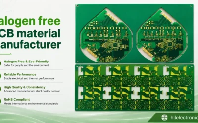
Halogen Free PCB Material Manufacturer for Compliant PCB Fabrication and Assembly
Halogen free PCB material manufacturing for compliant PCB fabrication, assembly, documentation, and traceability.
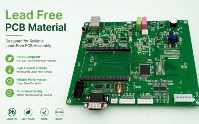
Lead Free PCB Material for PCB Assembly and Reliable PCBA Manufacturing
Lead free PCB material guidance for PCB assembly, reflow reliability, surface finish choice, and RoHS-ready PCBA.
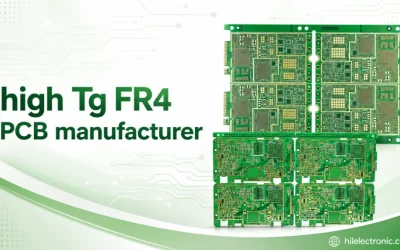
High Tg FR4 PCB Manufacturer for Industrial, Automotive, and Power Electronics
High Tg FR4 PCB manufacturing for industrial, automotive, and power boards with lead-free assembly and thermal stability.