
Global Electronic Components Sourcing Solutions
Source high-quality electronic components at competitive prices through Highleap’s global procurement network. We ensure cost-effective, timely, and traceable supply solutions for OEMs, EMS, and design houses worldwide.
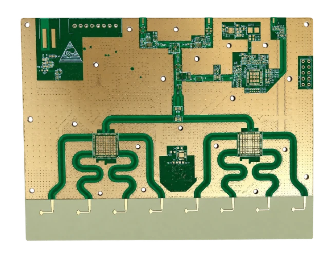
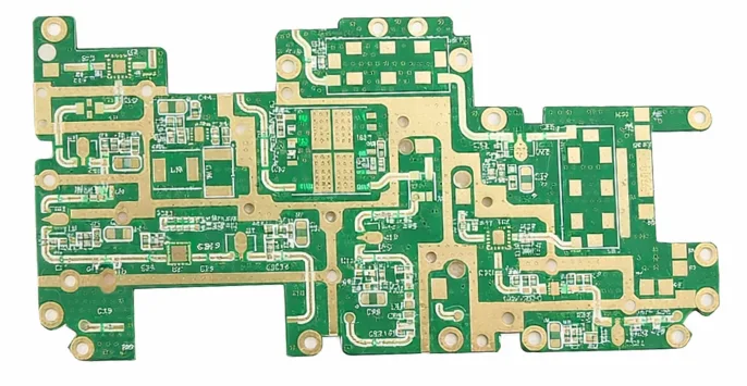
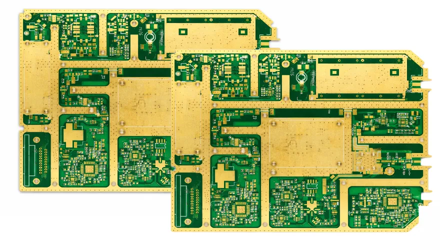
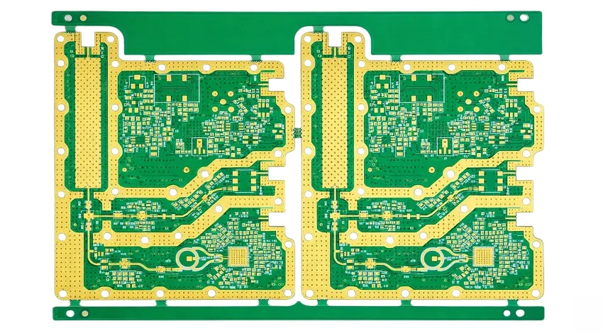
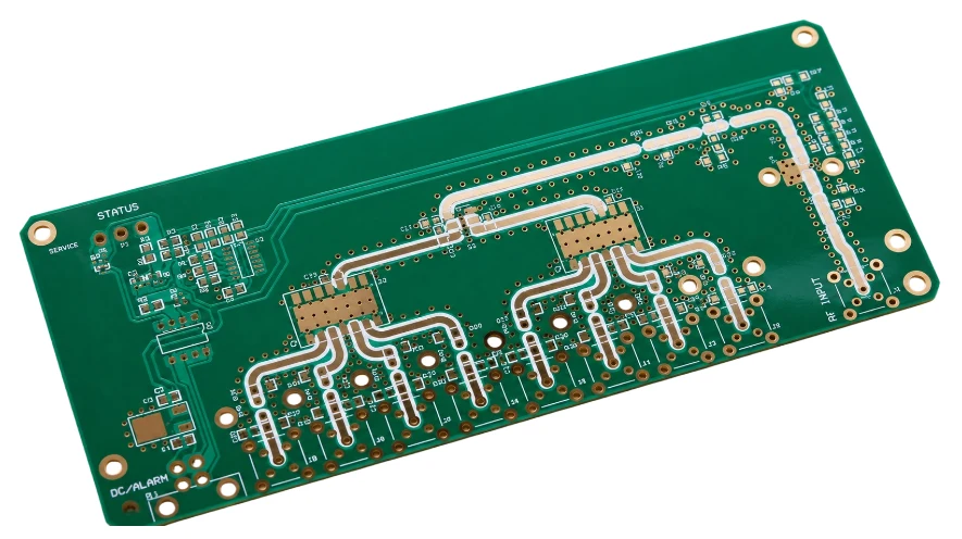

HIGH-FREQUENCY PCB MANUFACTURING
High-Frequency PCB Quote
Custom high-frequency PCB manufacturing for RF, microwave and high-speed electronic applications. Production is based on your Gerber files, stackup requirements, material selection and controlled impedance requirements.
Custom High-Frequency PCB
High-frequency PCB fabrication based on your Gerber files, layer count, board dimensions, stackup and manufacturing requirements.
RF & Microwave PCB
Custom RF and microwave PCB production for designs requiring controlled impedance, high-frequency routing and specialized material configurations.
High-Speed PCB Manufacturing
High-speed PCB production for electronic designs requiring controlled impedance and consistent manufacturing according to the approved stackup and layout.
High-Frequency Materials
Support for Rogers, PTFE and other high-frequency PCB material configurations according to the project design and material requirements.
Define the Right High-Frequency PCB for Your Design
High-frequency PCB requirements depend on the signal environment, material system, stackup and fabrication structure. Use the guide below to define the key requirements before quotation.
Choose the PCB Structure Around the Signal
RF & Microwave PCB
01RF and microwave boards require the PCB construction to support the required transmission-line characteristics. Material, dielectric thickness, copper characteristics, trace geometry and impedance should be considered together.
RF & Microwave PCB →High-Speed Digital + RF
02When RF and high-speed digital circuits share the same board, the stackup needs to accommodate both signal environments. Impedance, layer arrangement and material selection should be considered during fabrication planning.
High-Frequency PCB →Hybrid RF / Digital PCB
03Hybrid construction can combine high-frequency material with conventional PCB material when only selected layers require specific electrical characteristics. The material arrangement should be defined in the stackup.
Rogers PCB Stackup →Antenna & Microwave Structures
04Antenna and microwave boards depend on accurate RF geometry, dielectric configuration and copper features. These requirements should be included in the PCB design and fabrication data.
RF & Microwave PCB →Select the Material According to the PCB Requirement
Define the Parameters That Affect PCB Performance
Layer Count
State the total number of copper layers and identify whether the design uses a conventional multilayer or hybrid structure.
Controlled Impedance
Provide the required impedance values and, when available, identify the signal layers that require impedance control.
Dielectric Thickness
Provide the specified dielectric construction when the stackup and impedance depend on controlled dielectric thickness.
Copper Weight
Specify inner and outer layer copper requirements where different copper constructions are used.
Finished Board Thickness
Provide the target finished thickness and tolerance when the mechanical design depends on a specific board thickness.
Surface Finish
Specify the required surface finish when it has already been defined by the PCB or assembly requirements.
Identify Special Structures Before Quotation
Back Drilling
Identify back-drilled vias when via stubs need to be controlled for high-speed or RF signal paths.
Blind & Buried Vias
Indicate blind or buried via structures in the stackup and fabrication data when required by the routing design.
Hybrid Lamination
Specify which layers use high-frequency material and which use conventional PCB material in a hybrid construction.
Fine-Line RF Routing
Provide minimum trace width and spacing when fine-line RF structures are part of the PCB design.
Copper Requirements
Identify copper foil or surface requirements when copper characteristics are part of the electrical specification.
RF / Microwave Features
Include relevant RF geometry and fabrication notes in the Gerber, drawing or stackup package.
Ready to Quote Your High-Frequency PCB?
Share the information you have and we'll take it from there.
Send the project details that are currently available, such as PCB files, drawings, stackup, material requirements, quantity or other design information. You do not need to prepare every detail before requesting a quotation.
Our team will review the information provided and follow up if any additional details are needed. If design files are available, you can upload them directly with the quotation form.
Configure Your PCB
Choose the board construction, base material and fabrication requirements to get an instant indicative price range. Final pricing is confirmed after engineering review.
Take a Quick Quote
Ready to quote your next PCB project?
From prototype builds to high-volume production, Highleap supports multilayer PCB manufacturing, impedance control, quick engineering review and responsive quotation service for global customers.