
Rogers FR4 Hybrid PCB: Stackup, Cost & Process

Figure 1. Rogers-PCB, Rogers FR4 Hybrid PCB
A Rogers FR4 hybrid PCB places Rogers high-frequency laminate on the RF-critical layers and standard FR4 on the remaining layers — cutting material cost by 30–50% compared to an all-Rogers build while preserving RF performance where it matters. This guide covers hybrid stackup structures, material compatibility rules, lamination challenges, and manufacturing best practices for Rogers/FR4 mixed-dielectric PCBs.
Table of Contents
- What Is a Rogers FR4 Hybrid PCB and Why Use One
- Common Rogers FR4 Hybrid Stackup Configurations
- Material Compatibility: CTE, Dk, and Bonding
- Lamination Process for Rogers FR4 Mixed-Dielectric Boards
- Impedance Control in Hybrid Stackups
- Applications Driving Rogers FR4 Hybrid PCB Demand
- Manufacturing Rogers FR4 Hybrid PCBs at Highleap
1. What Is a Rogers FR4 Hybrid PCB and Why Use One
A Rogers FR4 hybrid PCB is a multilayer board that combines two different laminate families in a single stackup: Rogers high-frequency material (typically from the RO4000 series) on the layers carrying RF signals, and standard or high-performance FR4 on the layers handling digital routing, power distribution, and mechanical support.
The motivation is straightforward — cost versus performance. Rogers laminates offer low dielectric loss (Df typically 0.0037 for RO4350B at 10 GHz) and stable dielectric constant (Dk variation within ±2%), which are essential for maintaining signal integrity at GHz frequencies. But Rogers material costs 3–8× more than FR4 per panel, and not every layer in a multilayer PCB carries high-frequency signals. In a typical 6-layer mixed-signal design, only the top and bottom layers might route RF traces — the four inner layers handle power planes, ground planes, and low-speed digital signals that perform identically on FR4.
By using Rogers only where RF performance demands it and FR4 everywhere else, the hybrid approach achieves RF performance comparable to an all-Rogers board at a significantly lower material cost. For a 6-layer board, the material cost reduction is typically 30–50% compared to an all-Rogers construction. This makes Rogers FR4 hybrid PCBs the standard approach for cost-sensitive RF products in volume production — 5G radio units, automotive radar modules, Wi-Fi 6/7 access points, and satellite communication terminals.
The trade-off: hybrid stackups are more complex to manufacture than single-material boards. Different materials have different coefficients of thermal expansion (CTE), different lamination temperatures, and different adhesion characteristics. Managing these differences is the core manufacturing challenge.
2. Common Rogers FR4 Hybrid Stackup Configurations
Three hybrid stackup patterns cover the majority of Rogers FR4 PCB designs:
4-layer cap construction (Rogers outer, FR4 core). The most common hybrid configuration. Two Rogers cores (typically RO4350B or RO4003C, 10–20 mil thick) form the outer layers, bonded to a standard FR4 inner core with FR4 prepreg or Rogers 4450F bondply. Layer 1 and Layer 4 carry RF microstrip traces over ground planes on Layers 2 and 3, while the FR4 core handles DC power and low-speed control signals. Total board thickness: 1.0–1.6 mm. This stackup is symmetrical — essential for preventing warpage during lamination and reflow.
6-layer hybrid (Rogers outer, FR4 inner core). Extends the cap construction to 6 layers. Rogers on Layers 1 and 6, FR4 on Layers 2–5. The additional inner layers provide dedicated ground planes, power planes, and digital routing. Used in more complex mixed-signal designs where RF and digital sections coexist on the same board — 5G small-cell radios, phased-array antenna feed networks, and radar front-end modules with embedded processors.
Asymmetric hybrid (Rogers on one side only). Rogers on Layer 1 only, FR4 on all other layers. Lower cost than symmetrical cap construction but introduces a CTE asymmetry that can cause warpage. Suitable for simpler RF designs where only one surface carries microstrip traces — for example, a single-band power amplifier module. Board size should be kept small (typically under 100 × 100 mm) to manage warpage risk.
| Stackup | Rogers Layers | FR4 Layers | Typical Thickness | Cost vs All-Rogers | Warpage Risk |
|---|---|---|---|---|---|
| 4-layer cap (symmetric) | L1, L4 | L2, L3 core | 1.0–1.6 mm | 40–50% savings | Low |
| 6-layer cap (symmetric) | L1, L6 | L2–L5 core | 1.2–2.0 mm | 50–60% savings | Low |
| 4-layer asymmetric | L1 only | L2–L4 | 1.0–1.6 mm | 55–65% savings | Moderate |
| 8-layer hybrid | L1, L8 | L2–L7 core | 1.6–2.4 mm | 60–70% savings | Low |
Stackup symmetry is the most important rule for hybrid PCB reliability. A symmetrical layup (Rogers on both outer surfaces, FR4 in the center) balances the CTE mismatch across the board thickness, minimizing bow and twist during thermal cycling. PCB stackup design principles for impedance control and signal integrity apply to hybrid boards with additional constraints on material pairing.
3. Material Compatibility: CTE, Dk, and Bonding
The central engineering challenge of a Rogers FR4 hybrid PCB is making two different materials behave as one unified structure through lamination, soldering, and the product’s entire operating life. Three compatibility dimensions must be managed:
CTE (Coefficient of Thermal Expansion) matching. Rogers RO4000 series materials have X/Y CTE of 10–14 ppm/°C, while standard FR4 is 12–16 ppm/°C — a close enough match for reliable lamination. Z-axis CTE is more problematic: FR4 can exceed 50–70 ppm/°C above Tg, while RO4350B stays below 46 ppm/°C. This Z-axis mismatch stresses plated through-holes during thermal cycling. For hybrid boards with high via density, select a modified FR4 with low Z-axis CTE (such as IT-180A, Tg ≥ 175°C, or Panasonic Megtron 4) to reduce this mismatch.
Dk transition management. At the boundary between Rogers and FR4 layers, the dielectric constant changes abruptly — RO4350B has Dk = 3.48, while standard FR4 has Dk ≈ 4.2–4.5. Any signal via passing through this boundary experiences an impedance discontinuity. For RF signals, this creates reflections and insertion loss. Design mitigation: keep RF signal routing on Rogers layers only, and use vias only for ground stitching and power connections through the FR4 layers. If an RF signal must transition between Rogers and FR4 layers, surround the signal via with a tight fence of ground vias (spacing ≤ λ/20 at the operating frequency) to contain the impedance transition.
Bondply and prepreg selection. The adhesive layer between Rogers and FR4 must bond reliably to both materials. Rogers 4450F bondply (Dk = 3.54, 4 mil thick) is designed specifically for this purpose — it cures at temperatures compatible with both RO4000 and FR4. Alternative: high-resin-content FR4 prepreg (such as 1080 or 106 glass style) provides better adhesion to Rogers surfaces than standard 2116 prepreg due to higher resin flow. The bondply’s Dk must be accounted for in impedance calculations — it is a distinct dielectric layer in the stackup.

Figure 2. Rogers FR4 Hybrid PCB
4. Lamination Process for Rogers FR4 Mixed-Dielectric Boards
Lamination is where hybrid PCB manufacturing succeeds or fails. Rogers and FR4 have different thermal properties, and the lamination cycle must accommodate both.
Surface preparation. Rogers RO4000 series materials (hydrocarbon/ceramic composite) bond adequately with standard chemical cleaning. Rogers PTFE-based materials (RO3000, RT/duroid) require plasma treatment (CF₄/O₂ gas mixture) before lamination to activate the chemically inert PTFE surface and achieve reliable peel strength. Skipping plasma treatment on PTFE materials results in delamination — a pass/fail issue, not a gradual degradation. For RO4000-based hybrids, mechanical scrubbing or chemical micro-etching provides sufficient surface adhesion.
Lamination temperature profile. FR4 prepreg cures at 175–185°C. Rogers 4450F bondply cures at 190°C. The lamination cycle must bring both materials to their respective cure temperatures without over-curing the FR4 or under-curing the bondply. A stepped temperature profile — ramp to 175°C, hold, then ramp to 190°C for final cure — is standard practice. Pressure must be controlled to prevent excessive resin flow from the FR4 prepreg into the Rogers layer, which would distort the dielectric thickness and shift impedance.
Post-lamination cooling. Forced cooling for at least 2 hours after pressing relieves internal stress. Rapid cooling traps residual stress that manifests as warpage during subsequent reflow soldering. For boards thinner than 1.0 mm, controlled cooling is critical — thin hybrid boards are most susceptible to CTE-induced stress.
Drilling. Rogers ceramic-filled laminates are more abrasive than FR4 and wear drill bits faster. Drill spindle speed and feed rate must be adjusted — typically lower feed rate and higher spindle speed than FR4-only boards. Dedicated carbide drill bits rated for ceramic-filled substrates reduce hole wall roughness and improve subsequent copper plating adhesion. PCB drilling process parameters must be optimized for the hardest material in the stackup.
Desmear. Standard permanganate desmear works for FR4 layers but is inadequate for Rogers ceramic composites. Plasma desmear (using CF₄/O₂) is required to clean resin residue from hole walls at the Rogers layers, ensuring reliable copper-to-wall adhesion after electroless copper plating.
5. Impedance Control in Hybrid Stackups
Impedance control in a Rogers FR4 hybrid PCB requires treating each dielectric layer independently — there is no single “board Dk” for the entire stackup.
Field solver modeling. Standard impedance calculators that assume a uniform dielectric constant across all layers will produce incorrect results for hybrid boards. Use a 2D field solver (Polar SI9000, Ansys HFSS, or similar) that accepts different Dk values for each dielectric layer in the stackup. For microstrip on a Rogers outer layer, the Dk of the Rogers core determines the impedance. For stripline between FR4 layers, the Dk of the FR4 prepreg determines it. At boundaries where a signal via transitions between materials, model the impedance transition explicitly.
Copper roughness correction. At frequencies above 5 GHz, copper surface roughness significantly affects insertion loss. Rogers laminates are typically paired with low-profile (LP) or very low-profile (VLP) copper foil (Ra ≤ 1.5 µm) to minimize roughness loss. Standard FR4 uses electrodeposited (ED) copper with higher roughness. When modeling a hybrid stackup, apply the correct roughness correction factor for each layer — typically 1.2–1.5× for standard copper on FR4 layers, and 1.0–1.2× for LP copper on Rogers layers.
TDR validation. Every hybrid PCB production lot should include impedance test coupons that replicate the actual stackup — Rogers outer layer microstrip coupons and FR4 inner layer stripline coupons. TDR (Time Domain Reflectometry) measurements on these coupons validate that the fabricated impedance matches the designed target within ±5% (USB 3.x spec) or ±3% (RF spec, depending on application). Impedance-controlled PCB fabrication with TDR-verified coupons is standard practice for any hybrid board targeting RF or high-speed applications.
6. Applications Driving Rogers FR4 Hybrid PCB Demand
5G base station and small-cell radios. The RF front-end (power amplifier, low-noise amplifier, filters, antenna feed network) requires Rogers RO4350B or RO4003C for low insertion loss at 3.5–6 GHz (sub-6 GHz 5G) or 24–40 GHz (mmWave 5G). The digital baseband, power management, and network interface sections use FR4. A single hybrid PCB integrates both sections, replacing the older approach of separate RF and digital boards connected by cables.
Automotive radar (77/79 GHz). ADAS radar modules use Rogers RO3003 or RO4835 on the antenna and RF transceiver layers for low loss at 77 GHz, with FR4 inner layers for the radar processor, power supply, and CAN bus interface. The hybrid stackup must survive automotive thermal cycling (−40°C to +125°C) and meet AEC-Q100 qualification. Automotive radar PCB manufacturing requires hybrid material expertise combined with automotive quality processes.
Wi-Fi 6/7 access points. The RF transceiver section operates at 2.4 GHz and 5/6 GHz, where Rogers outer layers provide better impedance stability and lower loss than FR4. The SoC, Ethernet switch, PoE power section, and memory use FR4 inner layers. Hybrid construction keeps the BOM competitive for high-volume consumer networking products.
Satellite communication terminals. Ku-band (12–18 GHz) and Ka-band (26–40 GHz) flat-panel antennas and feed networks require ultra-low-loss Rogers or PTFE layers, while digital beamforming processors and power distribution use FR4. Board sizes can exceed 300 × 300 mm, making symmetric stackup design and CTE management critical to prevent warpage across the large panel.
7. Manufacturing Rogers FR4 Hybrid PCBs at Highleap
Highleap Electronics manufactures Rogers FR4 hybrid PCBs for telecommunications, automotive, aerospace, and industrial RF customers. Our hybrid PCB capability covers the full range of Rogers materials paired with standard and high-performance FR4:
Material pairing expertise. We stock Rogers RO4350B, RO4003C, and RO4835 cores in common thicknesses (8, 10, 20, 30, 60 mil), paired with matched FR4 cores (IT-180A, S1000-2M, or standard high-Tg FR4). Rogers 4450F bondply and high-resin 1080/106 FR4 prepreg available for interlayer bonding. Material recommendations provided during design review — we match CTE, Dk, and cure temperature for each application. Rogers PCB manufacturing at Highleap includes both all-Rogers and hybrid constructions.
Lamination and process control. Stepped-profile lamination press with in-situ temperature sensors for hybrid cure cycles. Plasma treatment capability for PTFE-based Rogers materials (RO3000, RT/duroid). Controlled post-press cooling to minimize residual stress. Registration accuracy ±50 µm across all layers.
Impedance validation. 2D field solver modeling for each hybrid stackup. TDR-verified impedance coupons on every production panel. Coupon-to-design correlation reports available on request. Impedance tolerance: ±5% standard, ±3% for precision RF applications.
Testing. Microsection analysis confirms via plating thickness (≥20 µm), interlayer registration, and bondline integrity. Ionic contamination testing (target ≤ 1.56 µg/cm²). VNA-based S-parameter measurement available for RF performance validation. High-frequency PCB fabrication testing methods ensure RF performance meets design targets.
Request a Rogers FR4 hybrid PCB quote — include your stackup design (or let us recommend one), Rogers material type, FR4 grade, impedance targets, board dimensions, and production volume.

Recommended Posts
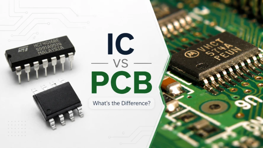
IC vs PCB: What’s the Difference and How They Work Together
Figure 1. IC vs PCB comparison showing the chip and the...

Electronic Reverse Engineering Service
You send us a physical PCB — or an electronic product...

High Frequency PCB Manufacturer China Selection Guide
Table of Contents China's HF PCB Manufacturing Capability...

Fast Turnaround Ceramic PCB Manufacturing
Table of Contents Why Most Turnaround Delays Originate on...
How to get a quote for PCBs
Let‘s run DFM/DFA analysis for you and get back to you with a report. You can upload your files securely through our website. We require the following information in order to give you a quote:
-
- Gerber, ODB++, or .pcb, spec.
- BOM list if you require assembly
- Quantity
- Turn time
For PCBA services, please provide your BOM (Bill of Materials) and any specific assembly instructions. We also offer DFM/DFA analysis to optimize your designs for manufacturability and assembly, ensuring a smooth production process.