

High-Speed RFSoC PCB Manufacturing and Assembly: Key Engineering Considerations
High-Speed RFSoC PCB Manufacturing and Assembly: Key Engineering Considerations
Get RFSoC PCBs manufactured with controlled impedance, reliable RF performance, high-density BGA assembly, and production-ready testing.
High-speed RFSoC hardware is difficult to manufacture for a simple reason: several sensitive functions are concentrated on one PCB. RF conversion, FPGA processing, GPU computing, DDR4 memory, high-speed links, storage and power conversion all have to work within the same electrical and mechanical structure.
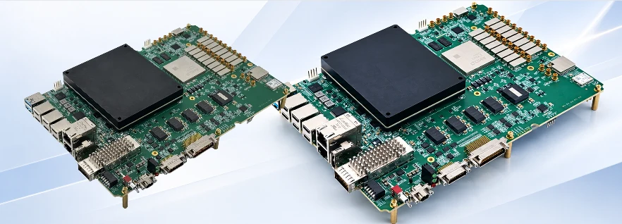
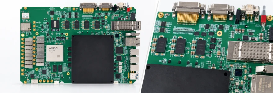
The five board views in this article show why fabrication and assembly should be reviewed as part of the engineering process. The front-side layout, labeled interfaces, backside storage area and overall board construction each reveal a different manufacturing consideration. The objective is not just to build the PCB, but to reproduce the design intent consistently in production.
What Makes RFSoC + GPU PCBs Different?
The board shown above combines two demanding processing domains. The RFSoC handles high-speed data conversion and programmable signal processing, while the Jetson AGX Orin provides GPU acceleration for compute-intensive workloads. Between them are memory, storage, power, clocking and high-speed communication functions. That concentration leaves less freedom to treat fabrication and assembly as separate from the original layout decisions.
For manufacturing, the important question is therefore not simply whether the PCB passes a design-rule check. Trace geometry, reference planes, via transitions, component clearances, copper distribution and thermal paths all have to remain practical when the design becomes a physical board.
On a mixed RF and high-speed compute board, a manufacturing review is most valuable before release to production. At that point, stack-up, fabrication tolerances and assembly strategy can still be adjusted without redesigning an already-built prototype.
Key Hardware Architecture of the RFSoC Platform
The platform is designed for demanding applications such as radar signal processing, high-speed communications, AI inference, electronic warfare research, SDR prototyping, and research or teaching. Its architecture combines wideband RF conversion with FPGA processing and GPU acceleration, so the PCB has to accommodate both sensitive analog/RF paths and dense digital interfaces.
The RF section uses an 8T8R architecture with stated channel isolation of at least 60 dB and SFDR of at least 55 dBc. Those figures make the physical PCB structure important. Laminate behavior, copper geometry, reference-plane continuity and connector transitions can all affect how the manufactured structure behaves compared with the intended design.
Interface placement is part of the PCB design
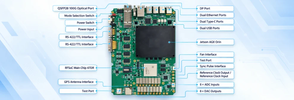
The labeled front view is useful because it shows that the external interface area is not simply a collection of connectors. High-speed ports such as the 100G QSFP28 and PCIe-related paths need controlled routing into the processing devices, while USB, Ethernet, DisplayPort, GPS and debug interfaces also need practical mechanical access.
The same principle applies to the Type-C debug interface with USB-to-JTAG and UART functions. A connector that is electrically correct but difficult to access during bring-up or production testing can slow the entire validation process. Interface placement should therefore be reviewed together with routing, enclosure constraints and test access.
For projects with comparable RF and high-speed requirements, Highleap's high-frequency PCB fabrication service can be relevant when impedance control, laminate selection and signal integrity become central manufacturing requirements.
PCB Manufacturing Considerations for RF and High-Speed Signals
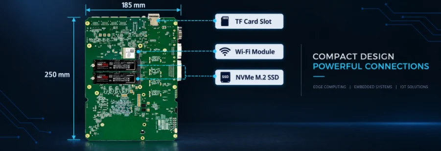
The board's backside view adds another important part of the manufacturing picture: the PCB has to fit the required mechanical envelope while still providing room for storage, routing, grounding and assembly access. This is especially important when high-speed components are placed on both sides of a relatively compact board.
Stack-up and controlled impedance
The physical dimensions shown in the board view are only part of the manufacturing constraint. For RF and high-speed nets, trace width, copper thickness, dielectric thickness and laminate properties determine the resulting impedance. These values should be agreed with the fabricator rather than assumed from a generic stack-up.
Highleap's PCB fabrication services support controlled-impedance and high-frequency builds. The important manufacturing question is whether the actual production stack-up can consistently reproduce the electrical assumptions used during layout.
Backside routing, storage and mechanical clearance
The backside NVMe area is a good example of why electrical and mechanical review should happen together. M.2 storage requires connector and module clearance, mounting support and access for assembly. At the same time, the surrounding copper and routing must preserve power, grounding and high-speed signal requirements.
The stated board size of 245 × 165 mm and 2.5 mm thickness also need to remain consistent with the enclosure, mounting points and connector positions. A production review should confirm these mechanical references before fabrication data is released.
Via structures and RF return paths
Every via creates a physical transition. On high-speed or RF paths, drill diameter, pad geometry, antipad dimensions and the return-current path can influence signal behavior. Ground stitching and reference-plane continuity are equally important around RF and high-speed transitions.
Copper distribution and thermal behavior
A board carrying an RFSoC, GPU, DDR4 and multiple high-speed interfaces also has significant power and thermal requirements. Copper distribution should therefore be checked for current carrying capability, power-delivery behavior, thermal paths and manufacturing balance rather than treated only as a routing problem.
A good production design is not simply one that a factory can build once. It is a construction that can be held within realistic process tolerances repeatedly while maintaining the electrical and mechanical characteristics required by the product.
Choose specialty processes only when the design needs them
A complex RFSoC board does not automatically require HDI, exotic laminates or ceramic construction. Those processes should be selected when routing density, frequency, thermal behavior or other verified requirements justify them. The fabrication process should follow the engineering requirement, not the other way around.
PCB Assembly Challenges for High-Density Components
The front-side PCBA view shows where fabrication decisions become an assembly problem. The RFSoC, GPU, memory, power devices, connectors and other components are concentrated into a limited area, leaving little room for uncontrolled placement or an assembly process that has not been planned around the layout.
Component placement cannot be separated from signal integrity
On a board like this, moving a component to improve assembly access can change a high-speed interconnect length, an RF path, a power path or the available thermal area. Placement therefore has to balance assembly access with the electrical requirements of the original design.
BGA and fine-pitch assembly
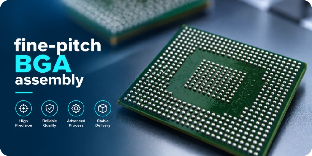
FPGA and processor packages concentrate many solder joints into a small area. Solder-paste printing, placement accuracy, reflow profile and board support all become important. Because many joints are hidden under BGA packages, X-ray inspection is an important complement to visual inspection and AOI.
Highleap's PCB assembly service supports SMT, through-hole and mixed-technology assembly with AOI, X-ray and functional testing. For a dense PCBA, the inspection strategy should be agreed before production rather than added after an assembly problem appears.
Thermal and mechanical assembly considerations
The GPU and RFSoC are not only high-value components; they are also major contributors to the board's thermal behavior. Solder quality, component coplanarity, thermal interfaces, heatsink or mechanical attachment and nearby component clearances can all affect the finished assembly.
Assembly documentation matters
A complete BOM, pick-and-place data, assembly drawing, polarity information, special process notes and test requirements give the manufacturing team a much clearer production target. For a complex PCBA, unclear documentation can create more production risk than the placement challenge itself.
If fabrication, component sourcing, SMT, through-hole assembly and testing need to remain coordinated through NPI and production, a turnkey PCB assembly workflow can reduce supplier handoffs.
Testing and Validation Before Delivery
The final board view should not be treated as proof that the PCBA is ready simply because all components are populated. A platform with RF conversion, FPGA processing, GPU computing, DDR4, PCIe, optical networking and multiple external interfaces needs a test plan that reflects those functions.
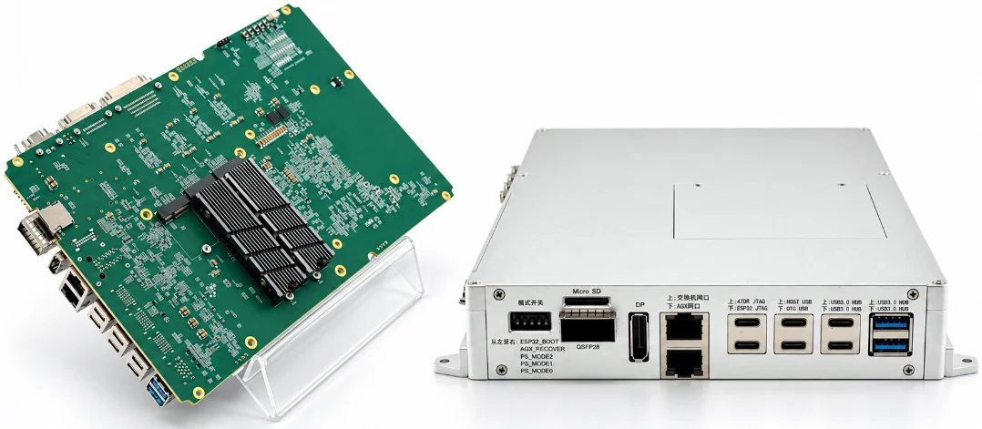
The Type-C interface with USB-to-JTAG and UART functions can support board bring-up and debugging. Test access should be considered during layout because connector accessibility, probe locations and test points become much harder to change after fabrication.
Testing should also be separated into appropriate stages. AOI and X-ray answer assembly questions; electrical testing checks basic connectivity; JTAG/UART supports bring-up; and functional or RF testing determines whether the completed board meets the intended system requirements.
Highleap's circuit board assembly workflow includes DFM review, component verification, inspection and testing. For high-speed electronics, defining test access and functional-test requirements early can make production validation much more efficient.
What to Review Before Sending a High-Speed PCB to Manufacturing
Before releasing a board like this, the engineering team should verify that the manufacturing package describes the physical and electrical requirements clearly enough for repeat production. The following checks are more useful than simply asking whether the Gerber files open correctly.
Recommended Quotation Package
For a meaningful manufacturing review, provide the PCB fabrication data, approved stack-up or impedance requirements, BOM, pick-and-place file, assembly drawing and any special RF, testing or inspection requirements. For a board with multiple high-speed interfaces, the relevant performance requirements are especially useful because they help the manufacturing team review the physical construction against the intended application.
If the project is still at prototype stage, Highleap also provides PCB prototyping support so the manufacturing process can be evaluated before moving into larger production quantities.
The board views and technical discussion in this article are presented for engineering and manufacturing reference. Customer-identifying information, proprietary schematics, Gerber files, BOMs and project-specific confidential details should not be published without authorization.
Highleap Electronics respects customer confidentiality and does not turn private customer design information into public marketing content without authorization.
From PCB Fabrication to Tested PCBA
For RFSoC, FPGA, GPU and other high-speed electronics, manufacturing works best when PCB fabrication, assembly, inspection and testing are considered early enough to influence the result.
Highleap Electronics supports complex PCB manufacturing and PCB assembly projects with engineering review focused on manufacturability, signal integrity, component assembly and production testing.
When requesting a quotation, providing the PCB data, BOM, assembly files and relevant performance requirements gives the engineering team the information needed to identify production risks before the first board is built.
Send Files & Get a QuoteRecommended Posts

Build to Print PCB Assembly Services
src="https://hilelectronic.com/wp-content/uploads/2026/08/PC...

Fine Pitch PCB Assembly Services for BGA, QFN & High-Density SMT
If you are sourcing fine pitch PCB assembly, the important...

HDI PCB Assembly | One-Stop HDI PCB Service
Figure 1. HDI PCB Assembly with Black Solder MaskHDI PCB...
Fine-Pitch BGA Assembly Services for High-Density PCBAs
If your released PCB already contains a fine-pitch BGA,...
How to get a quote for PCBs
Let’s run DFM/DFA analysis for you and get back to you with a report. You can upload your files securely through our website. We require the following information in order to give you a quote:
-
- Gerber, ODB++, or .pcb, spec.
- BOM list if you require assembly
- Quantity
- Turn time
For PCBA services, please provide your BOM (Bill of Materials) and any specific assembly instructions. We also offer DFM/DFA analysis to optimize your designs for manufacturability and assembly, ensuring a smooth production process.