
High Frequency PCB Fabrication Services

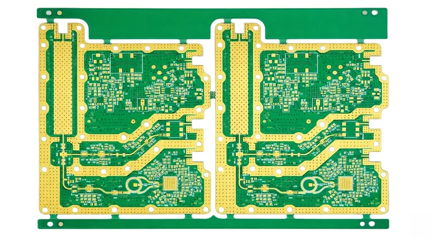
Highleap Electronics provides high frequency PCB fabrication services across the full spectrum of RF and microwave applications — from sub-6 GHz antenna modules and 5G mmWave arrays to 77 GHz automotive radar, satellite Ka/Ku-band hardware, and industrial RF test equipment. We fabricate with Rogers, Taconic, Isola, Panasonic Megtron, Nelco, and advanced hybrid stackup combinations. If your board operates above 1 GHz and demands controlled dielectric properties, low conductor loss, and verified impedance, we have the process infrastructure to deliver it.
Table of Contents
- High Frequency PCB Types We Fabricate
- High Frequency PCB Materials
- Fabrication Process Overview
- Hybrid Stackup and Lamination
- Etch Control and Copper Roughness
- Via Processing and Back-Drilling
- Solder Mask and Surface Finish
- Quality Testing and Verification
- Specifications by Application
- Highleap Fabrication Capabilities
1. High Frequency PCB Types We Fabricate
High frequency PCB is not a single product category — it describes any board where dielectric properties, conductor loss, and signal integrity above 1 GHz become primary design constraints. Highleap Electronics fabricates all of the following types:
|
PTFE-Based RF PCB
1 GHz – 100+ GHz
Rogers RO4000/RO3000 series, RT/duroid, Taconic TLX/TLY. The reference choice for microwave and mmWave where Dk stability and ultra-low Df are non-negotiable. |
Low-Loss Glass-Fiber PCB
1 GHz – 30 GHz
Panasonic Megtron 6/7, Isola I-Tera MT40, Nelco N4000-13EP. High-speed laminate platforms for RF and digital convergence at commercial scale. |
|
Ceramic-Filled Laminate PCB
5 GHz – 77+ GHz
Rogers RO3003, Taconic RF-35, Isola Astra MT77. Ceramic-loaded PTFE for tightly controlled Dk uniformity. Standard platform for 77 GHz automotive radar. |
Hybrid RF/Digital PCB
Multi-band, Mixed
Rogers or Megtron outer layers bonded with FR4 inner cores. Separates RF performance layers from digital layers to optimize cost without compromising signal integrity. |
|
Antenna PCB
0.8 GHz – 60 GHz
Patch antennas, phased arrays, slot antennas, MIMO. Fabricated on RO4350B, Megtron 6, or RO3003 depending on frequency, bandwidth, and gain requirements. |
Microwave / mmWave PCB
18 GHz – 100+ GHz
Power amplifiers, LNAs, mixers, filters at Ka, V, W-band. Requires HVLP copper, sub-mil trace control, and VNA-verified insertion loss on every production panel. |
|
RF Power Amplifier PCB
0.5 GHz – 6 GHz
High-current RF boards with mixed thermal and impedance requirements. Copper weight engineering, thermal via arrays, and controlled impedance on the same board. |
High-Speed Digital with RF Sections
SerDes, DDR5, PCIe 5
Megtron 6/7 or Nelco platform where SerDes, DDR5, or PCIe 5 signal integrity converges with RF front-end sections. Back-drilling and VLP copper standard. |
2. High Frequency PCB Materials
Material selection is the first and most consequential fabrication decision. The dielectric constant (Dk), dissipation factor (Df), and copper foil type together define what insertion loss and impedance tolerance your board can achieve. Highleap Electronics maintains qualified processes for all major high-frequency laminate families:
| Material | Family | Dk @ 10 GHz | Df @ 10 GHz | Freq. Range | Primary Use Case |
|---|---|---|---|---|---|
| RO4350B | PTFE/Ceramic | 3.48 ±0.05 | 0.0037 | DC – 40 GHz | 5G antenna, hybrid stackups, general microwave |
| RO4003C | PTFE/Ceramic | 3.55 ±0.05 | 0.0027 | DC – 40 GHz | Low-loss microwave, radar, satellite |
| RO3003 | PTFE/Ceramic | 3.00 ±0.04 | 0.0010 | DC – 77+ GHz | 77 GHz automotive radar, mmWave |
| RT/duroid 5880 | PTFE/Glass | 2.20 ±0.02 | 0.0009 | DC – 100+ GHz | Satellite Ka/Ku, defense, extremely low loss |
| Taconic TLY-5 | PTFE/Glass | 2.17 ±0.02 | 0.0009 | DC – 100+ GHz | Alternative to duroid 5880; microwave circuits |
| Taconic RF-35 | PTFE/Ceramic | 3.50 ±0.05 | 0.0018 | DC – 60 GHz | Antenna arrays, general RF |
| Megtron 6 | Low-loss Glass | 3.40 ±0.05 | 0.0038 | DC – 25 GHz | High-speed digital + RF convergence, 5G baseband |
| Megtron 7 | Low-loss Glass | 3.37 ±0.05 | 0.0030 | DC – 30+ GHz | Next-gen mmWave, high-density SerDes |
| Isola I-Tera MT40 | Low-loss Glass | 3.45 ±0.05 | 0.0031 | DC – 25 GHz | 5G infrastructure, backplane, RF amplifiers |
| Isola Astra MT77 | Low-loss Glass | 3.00 ±0.04 | 0.0017 | DC – 77+ GHz | 77 GHz radar on glass-fiber platform |
| Nelco N4000-13EP | Low-loss Glass | 3.70 ±0.05 | 0.0090 | DC – 15 GHz | RF/microwave, telecom infrastructure |
| FR4 High-Tg (Hybrid) | Standard Glass | 4.2–4.5 | 0.018–0.022 | Below 3 GHz | Inner cores in hybrid RF/digital stackups |
3. Fabrication Process Overview
A factory that runs high frequency boards through a standard FR4 line cannot produce consistent RF results. Highleap Electronics maintains dedicated process stations for HF-specific requirements at each stage:
- 1Inner layer imaging and etching — HF-compensated artwork scaling per material CTE; ±0.015 mm etch uniformity across panel
- 2AOI on all inner layers — automated optical inspection before lamination to eliminate buried defects
- 3Hybrid stackup layup — material-specific prepreg selection (RO4450F, FR4 1080/2116, or thermoplastic bond films depending on Dk requirements)
- 4Controlled lamination press cycle — temperature, pressure, and dwell profiles optimized per material combination; not shared with FR4 programs
- 5CNC drilling — controlled-depth drilling for back-drill programs; drill parameters adjusted per substrate hardness
- 6Plasma desmear (PTFE boards) — CF₄/O₂ vacuum plasma to remove PTFE smear; followed by sodium naphthenate activation for plating adhesion
- 7Electroless copper + electrolytic plating — via wall copper thickness verified by cross-section per IPC Class 2 or Class 3
- 8Outer layer precision etching — proactive etch compensation; trapezoidal etch factor measured per copper weight and applied to artwork
- 9Selective solder mask — LPI mask applied to component areas only; RF transmission lines left bare to prevent dielectric loading
- 10Surface finish application — Immersion Silver, ENIG, HASL, or OSP per application requirements
- 11Electrical test + TDR impedance coupon testing — 100% flying probe + TDR on every HF panel; VNA S-parameter testing available
- 12Final inspection, cross-section, and shipment — microsectioning on first articles and periodic production sampling; data retained and available on request
4. Hybrid Stackup and Lamination
Hybrid stackups — combining Rogers or Taconic outer layers with FR4 inner cores — are the most cost-effective architecture for boards that need RF performance on signal layers while tolerating standard material on power and digital layers. The fabrication challenge is thermal: RO4350B laminates at ~190°C while standard FR4 prepreg flows at 170–185°C. The bonding prepreg must achieve full adhesion to both surfaces within a single controlled press cycle.
| Bond Layer Option | Dk @ 10 GHz | Best Used With | Trade-off |
|---|---|---|---|
| Rogers RO4450F Prepreg | 3.52 | RO4000 series hybrid | Matched Dk to RO4350B; higher cost than FR4 prepreg |
| Standard FR4 Prepreg (1080/2116) | ~4.2–4.5 | Cost-driven hybrid builds | Dk mismatch at bond interface; higher insertion loss at bond layer |
| Thermoplastic Bond Film (e.g., FastRise 27) | 2.78 | PTFE-to-PTFE, PTFE-to-FR4 | Very low loss; requires tight temperature control |
CTE mismatch between PTFE/ceramic laminates and FR4 is compensated through anisotropic artwork scaling in CAM — layer-specific X/Y expansion offsets calculated per material before imaging. Highleap applies validated CTE compensation coefficients derived from in-house press characterization data, not generic estimates.
5. Etch Control and Copper Roughness
Etch Profile and Impedance Accuracy
Subtractive etching produces a trapezoidal trace cross-section — wider at the base, narrower at the top. For high-frequency boards, this profile shifts the effective impedance from the designed nominal. Highleap measures the etch factor for each copper weight and laminate combination, applies proactive artwork compensation, and maintains ±0.015 mm trace width uniformity across the panel.
Copper Roughness and Conductor Loss
At frequencies above 5 GHz, the skin effect concentrates current in the outer microns of the conductor. If copper surface roughness (Rz) exceeds the skin depth at operating frequency, current must follow the microscopic terrain of the copper surface — increasing effective path length, resistance, and insertion loss. Copper foil selection is therefore a primary loss engineering decision.
| Copper Foil Type | Rz (µm) | Loss vs. Standard ED | Target Frequency |
|---|---|---|---|
| Standard ED | 5.0–8.0 | Baseline | Below 3 GHz |
| Reverse-Treated (RTF) | 2.5–4.0 | ~25% lower | 3–15 GHz |
| Very Low Profile (VLP) | 1.5–2.5 | ~40% lower | 10–40 GHz |
| Hyper Very Low Profile (HVLP) | 0.8–1.5 | ~50% lower | 28 GHz – mmWave |
6. Via Processing and Back-Drilling
PTFE Plasma Desmear and Activation
PTFE laminates melt rather than fracture during CNC drilling, depositing a fluoropolymer smear layer on the hole wall that alkaline permanganate cannot remove. Highleap uses dedicated CF₄/O₂ vacuum plasma chambers to strip the fluorine atoms and eliminate smear. A sodium naphthenate etch activation step follows to render the chemically inert PTFE surface wettable for electroless copper seeding. Process parameters are validated by continuous destructive cross-section inspection. Standard chemical desmear lines are not used for PTFE boards.
Back-Drilling for Via Stub Elimination
Through-hole vias on multilayer HF boards create unused barrel segments — stubs — that resonate and create return loss notches in the frequency band. A 1.0 mm stub resonates at approximately 37 GHz. Highleap performs controlled-depth back-drilling to remove these stubs to ±0.1 mm depth tolerance. The residual stub length is calculated and provided to the RF designer for HFSS/CST model updates.
7. Solder Mask and Surface Finish
Selective Solder Mask
Standard LPI solder mask carries a Dk of 3.3–4.0 and Df of 0.02–0.03. Applied directly over an RF transmission line, it shifts impedance downward and increases insertion loss — sometimes enough to fail the loss budget at the board level. The correct approach is selective mask application: solder mask covers component pad areas, via rings, and non-RF surfaces only. RF transmission lines, antenna feeds, and ground plane windows are left bare. Highleap maintains ±0.05 mm mask registration for RF-selective clearance geometries.
Surface Finish Options for RF Boards
| Finish | Added Roughness | RF Loss Impact | Best For |
|---|---|---|---|
| Immersion Silver (ImAg) | 0.1–0.3 µm | Minimal | Best choice for loss-critical mmWave and microwave |
| OSP | Negligible | Negligible | Low-cost prototype; single reflow; short shelf life |
| ENIG | Low (Au layer) | Moderate above 5 GHz (Ni layer) | Wire bonding, multiple reflow, long shelf life |
| ENEPIG | Low | Lower than ENIG above 5 GHz | Wire bonding + RF coexistence; defense/aerospace |
| HASL (LF) | High (solder topology) | Not suitable above 3 GHz | Cost-driven non-RF sections only |
8. Quality Testing and Verification
TDR Impedance Coupon Testing — 100% Standard
Every production panel includes impedance test coupons reflecting the exact trace geometries of the board — single-ended, differential, coplanar waveguide as specified. All coupons are measured by Time Domain Reflectometry (TDR). Highleap provides the physical TDR data report with every shipment, not a binary pass/fail certificate.
VNA Insertion Loss Measurement
For applications where the insertion loss budget is the controlling specification — 5G mmWave, satellite Ka-band, 77 GHz radar — TDR alone is insufficient. Highleap offers Vector Network Analyzer (VNA) S-parameter measurement (S21, S11) up to operating frequency on production panels. VNA data is included in shipment documentation on request.
Cross-Section and Microsection Analysis
Destructive cross-sectioning verifies trapezoidal etch angles, plated copper wall thickness, Rogers-to-prepreg bond interface integrity, and PTFE plasma activation effectiveness. Cross-sections are performed on first articles and at defined production sampling intervals.
|
Impedance Tolerance
±5% / ±3%
Standard ±5%; ±3% available for critical RF nets with additional process controls |
Trace Width Uniformity
±0.015 mm
Panel-wide etch uniformity verified by periodic coupon measurement |
Back-Drill Tolerance
±0.1 mm
Controlled-depth back-drilling with residual stub length documentation |
9. Specifications by Application
| Application | Freq. Range | Typical Material | Impedance Tol. | Copper Foil | Key Fab Requirement |
|---|---|---|---|---|---|
| 5G Sub-6 GHz Antenna | 3.3–4.2 GHz | RO4350B hybrid / Megtron 6 | ±7% | RTF or Standard | Panel uniformity; volume consistency |
| 5G mmWave Array | 24–39 GHz | RO3003 / Astra MT77 | ±5% | VLP / HVLP | VNA verification; back-drilling; low Dk tolerance |
| 77 GHz Automotive Radar | 76–81 GHz | RO3003 / Astra MT77 | ±3–5% | HVLP | Dk uniformity ±0.02; IATF 16949; PPAP |
| Satellite Ka/Ku-Band | 12–40 GHz | RT/duroid 5880 / RO3003 | ±5% | VLP | IPC Class 3; full traceability; VNA data per panel |
| Wi-Fi 6E / UWB Module | 5–7 GHz | RO4350B hybrid / Megtron 6 | ±7–10% | RTF or Standard | Small board panelization; cost optimization |
| RF Power Amplifier | 0.5–6 GHz | RO4350B / Megtron 6 | ±5–7% | RTF | Thermal via arrays; mixed copper weight; controlled impedance |
| Defense / Aerospace Radar | 2–40 GHz | RT/duroid 5880 / RO3003 | ±3–5% | VLP / HVLP | IPC Class 3; MIL-PRF-31032; full material traceability |
| High-Speed Digital (RF Convergence) | SerDes / DDR5 / PCIe 5 | Megtron 6/7 / I-Tera MT40 | ±5–7% | VLP | Back-drilling; differential pair control; via stub modeling |
Submit Gerbers for HF PCB Quote →
10. Highleap Electronics High Frequency PCB Fabrication Services
Highleap Electronics operates as a full-service high frequency PCB fabrication and assembly partner. Our process infrastructure covers every material family and application type listed above, with dedicated equipment and process controls maintained specifically for RF and microwave boards:
- Material Qualification: Rogers RO4000/RO3000 series, RT/duroid 5880, Taconic TLX/TLY/RF-35, Megtron 6/7, Isola I-Tera MT40/Astra MT77, Nelco N4000-13EP, and hybrid FR4 combinations — all with validated press profiles.
- Hybrid Lamination: Thermodynamic press profiles validated for RO4350B/FR4, RO4003C/FR4, RO3003/FR4, and duroid 5880 stackups. Bond layer options include RO4450F, FR4 prepreg, and thermoplastic bond films.
- Copper Foil Engineering: Standard ED, RTF, VLP, and HVLP copper specified per-layer. RF signal layers matched to operating frequency loss budget.
- PTFE Plasma Processing: Dedicated CF₄/O₂ vacuum plasma desmear systems validated by continuous cross-section inspection. Not co-mingled with standard FR4 desmear lines.
- Precision Etch Control: ±0.015 mm panel-wide trace width uniformity; proactive etch compensation software applied per copper weight and laminate combination.
- Back-Drilling: ±0.1 mm stub depth tolerance; residual stub documentation provided for RF simulation model updates.
- Selective Solder Mask: RF-selective LPI application with ±0.05 mm registration; transmission lines and antenna structures left bare by default.
- Surface Finish Options: Immersion Silver, ENIG, ENEPIG, OSP — specified per application and reflow requirement.
- 100% TDR Testing: Impedance coupon TDR measurement on every HF panel. Physical data reports included with all shipments.
- VNA S-Parameter Testing: Available for loss-critical applications; S21/S11 data up to operating frequency.
- IPC Class 2 / Class 3: Full Class 3 capability for defense, aerospace, and medical applications including complete material traceability and microsection data packages.
- Integrated SMT Assembly: Seamless transfer to on-site turnkey assembly with HF-specific reflow profiles, preventing thermal shock to sensitive RF laminates.
Ready to fabricate your high frequency PCB? Send us your Gerbers and stackup requirements — we’ll return a DFM review, material recommendation, and fabrication quote.
Frequently Asked Questions
No. We fabricate high frequency PCBs on all major laminate families — PTFE-based (Rogers, Taconic, RT/duroid), ceramic-filled (RO3003, Astra MT77), low-loss glass-fiber (Megtron 6/7, I-Tera MT40, Nelco), and hybrid FR4 combinations. The right material is determined by your frequency range, loss budget, and cost requirements.
Standard FR4 becomes a liability above approximately 1–2 GHz for loss-sensitive RF traces. For controlled impedance structures above 3 GHz, we recommend low-loss glass-fiber laminates (Megtron 6) as a minimum. For designs above 10 GHz, PTFE or ceramic-filled PTFE is the industry standard.
Yes — hybrid RF/FR4 stackups are a standard product at Highleap. We maintain validated press profiles for RO4350B/FR4, RO4003C/FR4, and RO3003/FR4 combinations with both RO4450F and standard FR4 prepreg bonding options.
TDR impedance coupon data is included as standard with every high frequency PCB shipment. VNA S-parameter measurement (S21/S11) is available on request for applications with insertion loss specifications.
Yes. We fabricate 77 GHz automotive radar PCBs on RO3003 and Astra MT77 with IATF 16949 process controls, PPAP documentation capability, Dk uniformity verification, and HVLP copper foil as standard. Contact us to discuss APQP requirements.
We support prototype quantities from a single panel through full production volumes. RF and microwave boards are accepted at any quantity — contact us with your Gerber files and stackup for a specific quote.

Recommended Posts

Wireless Mechanical Keyboard PCB Manufacturing
Table of contentsWireless Keyboard PCB Procurement...

Split Keyboard PCB Manufacturing & Assembly
Table of contentsSplit Keyboard PCBA Procurement...
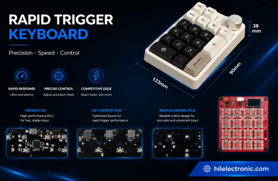
Rapid Trigger Keyboard PCB Manufacturing & PCBA
Table of contentsRapid Trigger PCBA Buying and Performance...
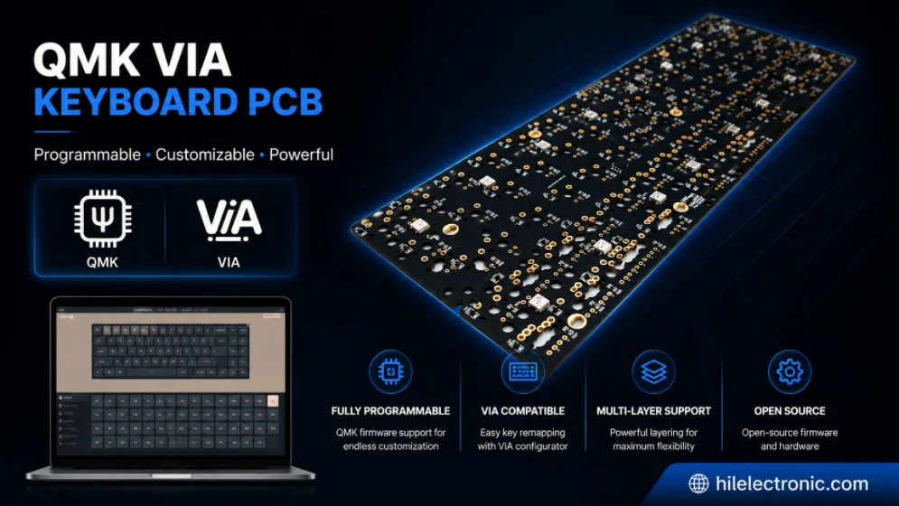
QMK/VIA Keyboard PCB Manufacturing & Assembly
Table of contentsQMK/VIA Keyboard PCB Buying...
How to get a quote for PCBs
Let us run DFM/DFA analysis for you and get back to you with a report.
You can upload your files securely through our website.
We require the following information in order to give you a quote:
-
- Gerber, ODB++, or .pcb, spec.
- BOM list if you require assembly
- Quantity
- Turn time