
Fast High Frequency PCB Manufacturing

However, accelerating high-frequency (HF) board production is fundamentally different from expediting standard FR4. Pushing PTFE or hydrocarbon ceramic laminates through a factory faster requires manipulating thermodynamic profiles, chemical etching kinematics, and dimensional scaling. This guide dismantles the factory-floor realities of fast high frequency PCB manufacturing, separating the steps you can compress from the physics you cannot cheat.
Key Takeaways
Compressing high-frequency PCB lead times is an exercise in managing material rheology and chemical inertness. Highleap Electronics achieves 5-7 day turnarounds on Rogers hybrid stackups not by rushing chemistry, but by utilizing dedicated PTFE plasma chambers, pre-stocked low-loss laminates, and advanced Laser Direct Imaging (LDI) to bypass traditional processing bottlenecks.
Submit Gerber for HF PCB Quote
1) Common Scenarios for Fast High-Frequency PCB Manufacturing
1.1 Prototype Validation (Functional Testing)
When the objective is strictly proof-of-concept for an RF topology, hardware engineers can often relax certain mechanical constraints to buy time. Widening impedance tolerances from ±5% to ±10% allows the CAM department to skip sequential etching passes and complex TDR launch pad modeling, shaving critical hours off the front-end engineering timeline without compromising the core functional demonstration.
1.2 Design-In Competition (Time-to-Market)
In socket competitions, hardware must be both fast and close to production-intent. The optimal strategy here is concurrent engineering. Submit preliminary routing (70-80% complete) for initial DFM review. This allows the factory to lock in X-Y dimensional scaling factors (critical for PTFE materials) and pull specific prepreg styles from inventory while you finalize the remaining RF traces.
1.3 Regulatory Certification (FCC/CE/EMC)
Certification builds permit zero deviation. Insertion loss, skin effect mitigation, and precise Dk/Df matching must reflect final mass production. In this scenario, acceleration can only occur through priority machine scheduling (queue jumping) and premium logistics. Attempting to compress lamination dwell times or desmear cycles here will result in micro-voids or Dk drift, causing the board to fail the very emissions tests you are rushing to pass.
2) High-Frequency PCB Lead Times vs. Standard FR4
Understanding the baseline processing times is crucial for setting realistic expectations. High-frequency boards simply require more machine time than standard consumer electronics boards.
| Process Phase | Standard 4L FR4 (Rush) | 4L Rogers Hybrid (Rush) | 4L Pure PTFE (Rush) | The Engineering Bottleneck |
|---|---|---|---|---|
| CAM & Tooling | 2–4 hrs | 4–8 hrs | 6–12 hrs | Calculating aggressive anisotropic X-Y shrinkage rates unique to PTFE matrix materials. |
| Lamination (Press) | 3–4 hrs | 5–7 hrs | 8–12 hrs | Asymmetric CTEs in hybrids require highly controlled thermal ramping to prevent internal shear stress and warp. Pure PTFE requires high-temp fusion bonding (>390°C). |
| CNC Drilling | 1–2 hrs | 2–4 hrs | 4–6 hrs | Strict limitation on drill hit counts (often <200 hits) to prevent ceramic filler from destroying carbide bits and causing via wall tearing. |
| Desmear & Activation | 4–6 hrs | 6–10 hrs | 10–16 hrs | Standard permanganate fails on PTFE. Requires complex CF4/O2/N2 plasma gas mixtures or hazardous sodium naphthalene treatment. |
| Imaging & Etching | 2–4 hrs | 4–6 hrs | 4–8 hrs | LDI and specialized etching profiles to minimize copper surface roughness (Rz) degradation, preserving insertion loss characteristics. |
| Minimum Fab Time | ~24 hrs | ~36–48 hrs | ~48–72 hrs | (Excludes raw material procurement and outbound logistics) |
3) How Material Availability Impacts PCB Turnaround Time
The fastest fabrication process in the world cannot start without the substrate on the factory floor. The foundation of any RF board is its PCB laminate material. For fast-turnaround projects, the difference between a 5-day delivery and a 5-week delay entirely depends on your material selection strategy and understanding of base chemistry.
3.1 PTFE vs. Hydrocarbon Ceramic: The Speed Trade-off
When selecting high frequency materials, engineers generally choose between two primary resin systems, each with drastically different lead times and processing challenges:
- Ceramic-filled PTFE (e.g., Rogers RO3000® Series): Polytetrafluoroethylene (PTFE) offers the ultimate low dissipation factor (Df) for 77GHz automotive radar and aerospace telemetry. However, PTFE is inherently soft (leading to “cold flow” registration issues) and chemically inert. It requires extensive plasma desmear cycles and specific fusion lamination temperatures. If your specified PTFE laminate is not in the factory’s inventory, importing it can add 3 to 5 weeks to your lead time.
- Hydrocarbon Ceramic Thermosets (e.g., Rogers RO4000® Series): Materials like RO4350B and RO4003C were explicitly engineered to bridge the gap between high-frequency performance and FR4-like manufacturability. Because they do not require plasma desmear or exotic lamination profiles, they process much faster. Crucially, top-tier manufacturers typically stock these materials in high volumes, making them the absolute best choice for expedited prototypes.
3.2 Strategic Dielectric Substitutions for Accelerated Lead Times
If your specified material is out of stock, standing still is not an option. Experienced RF designers utilize strategic material substitution to keep the project moving. If you need a board in 7 days, consider these compromises:
- RO4003C vs. RO4350B: If RO4003C (Dk 3.38, Df 0.0027) is unavailable, RO4350B (Dk 3.48, Df 0.0037) is often a viable substitute for sub-15GHz applications. RO4350B is highly stocked due to its UL 94V-0 flame retardant rating. A quick recalculation in your 2D field solver to adjust trace widths by a fraction of a mil can save you weeks of waiting.
- Managing Copper Foil Profiles: High-frequency designers often specify Rolled Annealed (RA) copper or Reverse Treated Foil (RTF) to mitigate skin-effect losses at millimeter-wave frequencies. However, standard Electrodeposited (ED) copper is far more readily available. If the prototype is intended for digital logic validation or sub-6GHz testing, downgrading to ED copper temporarily can bypass severe supply chain bottlenecks.
3.3 The Power of Hybrid Stackups
You do not need expensive, hard-to-source PTFE on all 10 layers of a board. A highly effective strategy for both cost reduction and speed is the hybrid stackup. By utilizing low-loss high frequency materials exclusively on the outer RF signal layers (L1-L2), and standard High-Tg FR4 for internal digital logic and power distribution planes, you dramatically simplify the supply chain. This approach allows the factory to pull from standard FR4 inventory for 80% of your board’s volume.
4) Mandatory Processing Steps for High-Frequency PCBs
4.1 Rheology and Lamination Dwell Times
Resin flow characteristics (rheology) cannot be rushed. High-frequency thermosets and thermoplastic PTFEs require precise melt viscosities to fill gaps between copper traces without displacing the glass weave. Accelerating the thermal ramp rate creates trapped volatiles (causing delamination during lead-free reflow) or induces anisotropic stress that permanently alters the localized Dielectric Constant (Dk). The press cycle takes the time the chemistry demands.
4.2 Breaking the Carbon-Fluorine Bond (Desmear)
PTFE is incredibly chemically inert. Standard alkaline permanganate desmear lines, used for FR4, will simply bead up and roll off a PTFE via wall. To achieve copper plating adhesion, the fluorine atoms must be stripped from the carbon backbone. This requires placing the panels in a vacuum plasma chamber with a specific CF4/O2 gas mixture for an extended cycle. Skipping or shortening this step guarantees catastrophic via barrel cracking under thermal shock. Highleap Electronics maintains dedicated plasma lines exclusively for HF materials to prevent queue bottlenecks.
5) How to Avoid Delays in High-Frequency PCB Production
The most devastating delays in rush orders occur before the board ever hits the factory floor. Engineering holds (EQs) consume days. To bypass this, your data package must proactively address HF-specific manufacturing realities.
- Target Operating Frequency: Dk is not static; it shifts with frequency. Do not just specify “Dk 3.5.” Specify “Design Dk 3.55 @ 10GHz” so the CAM team utilizes the correct dielectric model for impedance calculations.
- Explicit Stackup Construction: Define the exact prepreg types, core thicknesses, and copper foil types. For complex routing involving micro-vias, ensure your documentation aligns with standard HDI PCB design rules to prevent CAM rejections.
- Pre-Authorize Etch Compensation: Add a fabrication note: “Manufacturer authorized to adjust trace widths up to ±1 mil to hit impedance targets without submitting EQ.” This eliminates a 24-hour approval round-trip.

6) Quality Assurance and Testing for Fast Turnaround PCBs
6.1 Targeted Verification for High-Frequency Designs
Standard visual inspection is insufficient for mmWave or high-speed digital boards. Quality assurance must be targeted to protect signal integrity:
- TDR Impedance Verification: Single-ended, differential, and coplanar waveguide structures must be measured via Time Domain Reflectometry (TDR) on custom-designed test coupons at the panel edge.
- Microsectioning (Cross-Section): Vital for evaluating plating thickness in high-aspect-ratio vias and ensuring zero resin recession after the aggressive plasma desmear cycle.
For functional prototypes where absolute longevity is secondary to immediate electrical performance, destructive testing can be deferred, but TDR measurement remains an absolute non-negotiable step.
7) Fast High-Frequency PCB Manufacturing Services
Highleap Electronics engineers its fast-turnaround infrastructure to eliminate administrative queue times while rigidly enforcing the metallurgical and chemical requirements of advanced substrates. For a deep dive into our end-to-end capabilities, review our complete PCB manufacturing process.
- Predictive Inventory: We continuously stock Rogers RO4000 series, RT/duroid, and Panasonic Megtron laminates in standard thicknesses to neutralize supply chain lead times.
- Laser Direct Imaging (LDI): We bypass traditional photo-tooling, utilizing LDI to achieve precise ±15µm trace width tolerances, crucial for edge-coupled filters and millimeter-wave antennas.
- Dedicated HF Process Lines: By isolating PTFE drilling, plasma desmear, and specialized lamination presses from our standard FR4 volume, your rush order never waits behind commercial production batches.
- Seamless Turnkey SMT: Bare boards transition immediately to our SMT assembly floor. We employ specific multi-zone reflow profiles tailored to the CTE and thermal mass of advanced hybrid stackups, preventing assembly-induced warpage.
For a complete data package utilizing stocked low-loss laminates, Highleap routinely delivers fabrication in 5–7 business days. Submit your Gerber and stackup files today for an immediate engineering DFM review.

Recommended Posts

Wireless Mechanical Keyboard PCB Manufacturing
Table of contentsWireless Keyboard PCB Procurement...

Split Keyboard PCB Manufacturing & Assembly
Table of contentsSplit Keyboard PCBA Procurement...
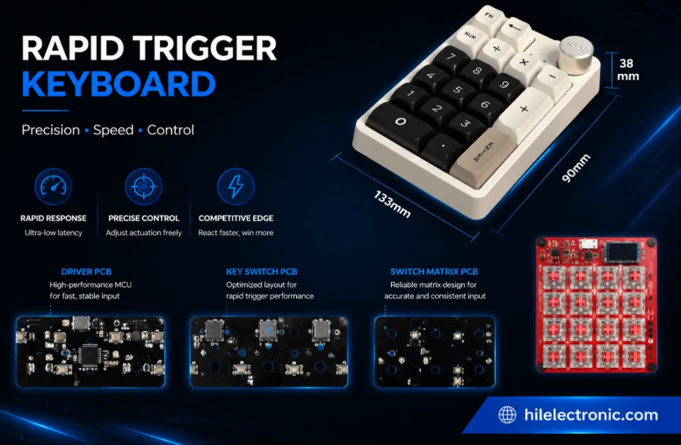
Rapid Trigger Keyboard PCB Manufacturing & PCBA
Table of contentsRapid Trigger PCBA Buying and Performance...
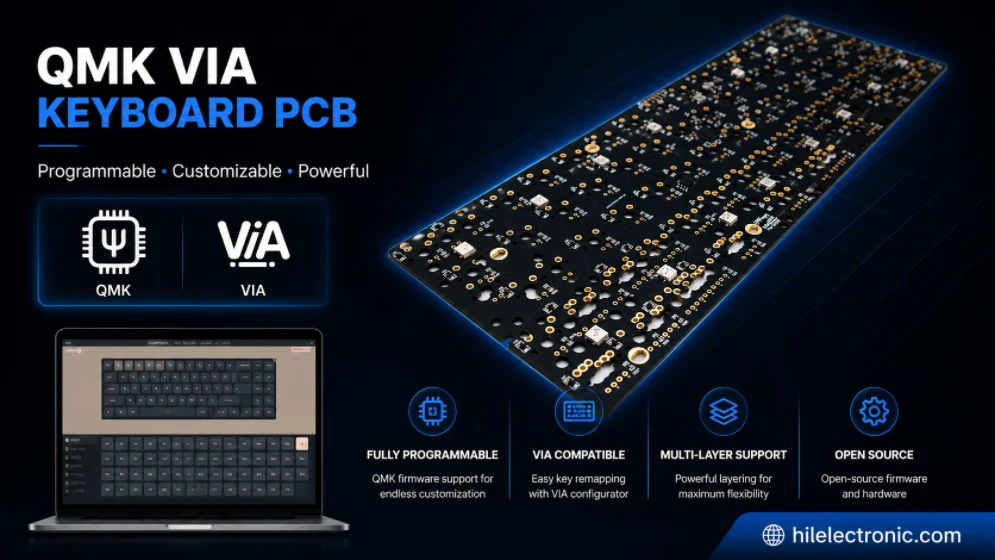
QMK/VIA Keyboard PCB Manufacturing & Assembly
Table of contentsQMK/VIA Keyboard PCB Buying...
How to get a quote for PCBs
Let us run DFM/DFA analysis for you and get back to you with a report.
You can upload your files securely through our website.
We require the following information in order to give you a quote:
-
- Gerber, ODB++, or .pcb, spec.
- BOM list if you require assembly
- Quantity
- Turn time