
Mobile PCB Fabrication and Assembly

Smartphone PCBs are among the most demanding circuit boards manufactured at scale—10 to 12 copper layers compressed into under 1mm of thickness, carrying signals from DC power rails to 40GHz 5G antenna feeds simultaneously. Manufacturing them reliably requires a different class of equipment, process control, and engineering support than standard commercial PCB production.
Highleap Electronics specializes in mobile PCB fabrication and assembly for OEM and ODM customers, handling everything from early engineering samples to high-volume production runs under one roof. Our phone circuit board manufacturing capability covers the full range of current smartphone platform requirements.
What Makes a Mobile PCB Different from Standard PCBs
A mobile PCB—also called a smartphone PCB, phone circuit board, or mobile phone motherboard—is not simply a small version of an industrial or consumer electronics board. The combination of constraints it must meet simultaneously is found nowhere else in electronics manufacturing.
Layer counts run 10–12 versus the 2–6 typical of standard commercial boards. Total board thickness must stay at or below 1.0mm. Minimum trace width is 50μm (2 mil) compared to 100–150μm on standard boards. Via technology shifts from mechanical through-holes to HDI laser micro-vias at 0.1mm drill diameter. And signal frequencies reach up to 40GHz for 5G mmWave—versus typically below 1GHz on standard boards.
These constraints compound each other. Fitting 1,000–1,500 components into a board smaller than a credit card while maintaining 5G RF isolation, thermal paths for a 10W SoC, and LPDDR5X memory routing at 8,533 Mbps requires fabrication and assembly processes that most PCB factories simply cannot support.
HDI Technology: Why Smartphones Need It
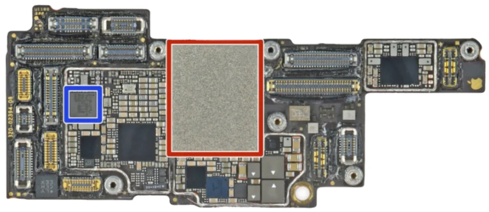
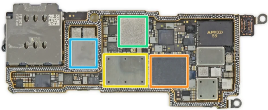
High Density Interconnect (HDI) PCB technology is not optional in modern smartphone design—it is the only fabrication approach that supports current SoC package densities. A flagship application processor in a 0.4mm pitch BGA package cannot be routed using conventional through-hole via technology; there is not enough physical space on the inner layers to fan out the signal traces.
HDI solves this by replacing large mechanical vias with laser-drilled micro-vias (0.1mm diameter) that connect only the layers they need to, leaving inner layer routing space available. Stacked micro-via structures—where multiple blind vias are built up vertically through sequential lamination cycles—enable the escape routing density that modern mobile SoC packages require.
Build-up configuration is determined by the SoC package pitch and interface count: 1+N+1 (6–8 layers) for mid-range smartphones; 2+N+2 (8–10 layers) for flagship SoC integration; ELIC 3+N+3 (10–12 layers) for 5G mmWave flagships. For fabrication specifications and cross-section qualification methods, see Highleap Electronics’ HDI PCB manufacturing page.
What to Look for in a Mobile PCB Manufacturer
Not every PCB factory that lists HDI capability can actually produce mobile-grade boards at yield rates that make volume production viable. When qualifying a mobile PCB supplier, four things separate capable manufacturers from ones that will generate respins:
- Laser drill at 0.1mm minimum — micro-via diameter directly limits BGA routing density; factories limited to 0.15mm drill cannot support current flagship SoC packages
- Impedance control with TDR verification — simulation-only impedance is insufficient for 5G RF and LPDDR5X memory interfaces; measured coupon data must ship with every production lot
- 100% AXI on BGA packages — automated X-ray inspection of every joint is the only way to catch void percentages before boards reach functional test; sampling is not adequate for mobile production
- Fabrication and assembly under one roof — split-vendor supply chains introduce reflow profile mismatches and accountability gaps when yield problems appear
Highleap Electronics: Mobile PCB Fabrication and Assembly
Highleap Electronics manufactures mobile PCBs for smartphone OEMs and ODMs building on Qualcomm Snapdragon, MediaTek Dimensity, and Samsung Exynos platforms.
| Capability | Specification |
|---|---|
| Layer Count | Up to 12 layers; ELIC 3+N+3 stack-ups |
| Minimum Trace / Space | 2/2 mil (50μm) |
| Laser Micro-Via | 0.1mm minimum; copper-filled stacked vias |
| Impedance Control | ±8%; TDR coupon data with every production lot |
| Materials | Modified FR4, Rogers RO4000, LCP — per-layer selection for hybrid 5G designs |
| Surface Finish | ENIG, ENEPIG, OSP |
| SMT Placement Accuracy | ±15μm; 01005 passives and 0.3mm pitch BGA as standard |
| Reflow | Nitrogen atmosphere; profile developed per board design |
| Inspection | 100% flying probe (bare board); 100% AXI on all BGA/QFN (assembly) |
| Certifications | ISO 9001:2015; IPC-A-610 Class 2 |
For 5G sub-6GHz and mmWave designs, we specify Rogers RO4000 or LCP on RF layers—the same low-loss material specifications used across our high frequency PCB production line. We also manufacture rigid-flex boards for camera modules and foldable hinge interconnects, and wireless charging PCBs for Qi assemblies—covering the full PCB scope of a modern smartphone in a single supply relationship.
Mobile PCB Prototype to Mass Production: How the Process Works
Most mobile PCB projects start with a Gerber file review. A Gerber set, a rough stack-up specification, and expected volumes are enough to get a DFM report and preliminary quote within 24–48 hours. Engineering sample builds typically run 7–14 days for bare board, with 3–5 days added for assembled prototype. Design qualification follows—X-ray cross-section, impedance validation, thermal cycle sampling—before volume production locks process parameters. For a full overview of how boards move through our factory, see our PCB manufacturing process page.
We support both turnkey (we source components) and consigned-material assembly. For customers moving from another supplier, we offer a free DFM review of existing designs—this often identifies the root cause of yield issues that were previously attributed to design.
Frequently Asked Questions About Mobile PCB Manufacturing
How many layers does a smartphone PCB typically have?
Most modern flagship smartphones use 10–12 layer PCBs. Mid-range devices typically use 6–8 layers. The layer count is driven by the SoC platform: Qualcomm Snapdragon 8-series and MediaTek Dimensity 9000-series designs generally require 10+ layers to route all high-speed interfaces without signal integrity compromises.
What is the minimum order quantity for mobile PCB fabrication?
Highleap Electronics has no minimum order quantity for prototype builds. Engineering sample runs of 5–20 boards are common starting points. Volume production pricing applies from approximately 500 units, with full mass production optimization available from 5,000 units and above.
What files do I need to submit for a mobile PCB quote?
Gerber files (RS-274X format) and a stack-up specification are sufficient to get started. A BOM is required for assembly quotes. We can work with ODB++ files, and our engineering team will request any missing information during the DFM review—you don’t need a complete package to begin the conversation.
Can you manufacture mobile PCBs that support 5G mmWave?
Yes. 5G mmWave designs require low-loss dielectric materials (Rogers RO4000 or LCP) on RF layers, with controlled impedance traces verified by TDR measurement. We manufacture hybrid stack-ups combining these materials with standard FR4 on inner layers, and validate RF section impedance with coupon data delivered with every production lot.
What certifications does Highleap Electronics hold for mobile PCB production?
Highleap Electronics is ISO 9001:2015 certified and produces to IPC-A-610 Class 2 as baseline. IPC Class 3 inspection criteria are available on request for projects with elevated reliability requirements. All production lots ship with full traceability documentation including material lot records, inspection reports, and impedance test data.

Recommended Posts

Wireless Mechanical Keyboard PCB Manufacturing
Table of contentsWireless Keyboard PCB Procurement...

Split Keyboard PCB Manufacturing & Assembly
Table of contentsSplit Keyboard PCBA Procurement...
Rapid Trigger Keyboard PCB Manufacturing & PCBA
Table of contentsRapid Trigger PCBA Buying and Performance...
QMK/VIA Keyboard PCB Manufacturing & Assembly
Table of contentsQMK/VIA Keyboard PCB Buying...
How to get a quote for PCBs
Let us run DFM/DFA analysis for you and get back to you with a report.
You can upload your files securely through our website.
We require the following information in order to give you a quote:
-
- Gerber, ODB++, or .pcb, spec.
- BOM list if you require assembly
- Quantity
- Turn time