
Phone Circuit Board Manufacturing and HDI Assembly

Every smartphone depends on a phone circuit board engineered to tolerances measured in microns—a multi-layer laminated assembly where copper pathways thinner than a human hair carry signals between hundreds of components at frequencies from DC power to millimeter-wave 5G. At Highleap Electronics, we manufacture phone circuit boards for OEM and ODM customers worldwide, combining 12-layer HDI fabrication with full SMT assembly under one ISO 9001–certified roof. This guide covers what’s inside a modern phone circuit board, why mobile manufacturing tolerances are so demanding, and what separates a qualified supplier from one that will cost you failures in the field.
Whether you’re a hardware engineer planning your first HDI tape-out, a procurement team qualifying a new PCB partner, or an ODM moving from design to production—the manufacturing realities here apply directly to your decisions.
Contents
Anatomy of a Phone Circuit Board
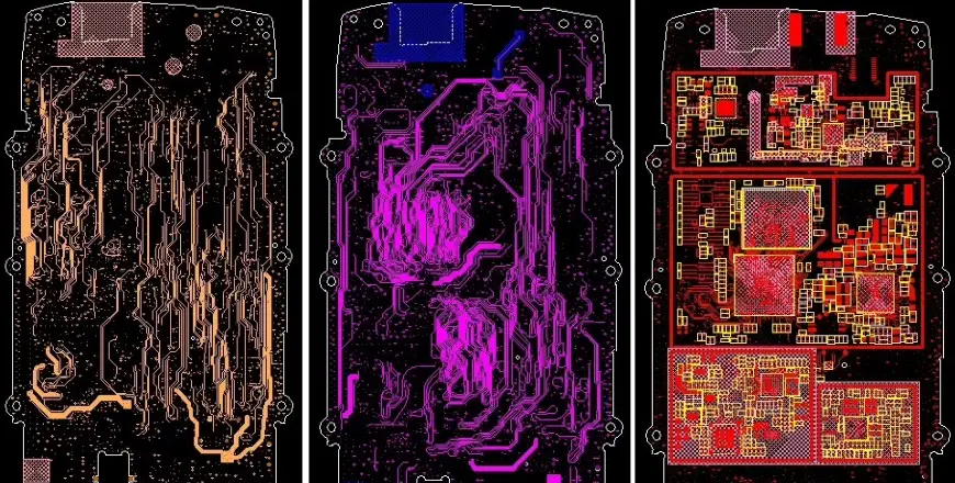
A phone circuit board is not a flat plate with chips attached. It is a precision laminated structure with 10 to 12 copper layers, total thickness below 1.0mm, carrying signals from DC power rails to 40 GHz RF simultaneously. Each layer serves a specific electrical role—signal routing, power distribution, ground plane for EMI suppression, or RF antenna feed—and these layers interact electromagnetically: a decision on Layer 4 affects signal behavior on Layer 7 at 5 GHz.
Manufacturing Insight
The stack-up design—chosen before any trace is routed—determines the board’s electromagnetic performance ceiling and its manufacturing cost. Revising the stack-up after routing begins is among the most expensive mistakes in mobile PCB development.
The Substrate: Foundation of All Electrical Performance
High-end phone circuit boards use modified FR4 laminates for digital sections and low-loss materials (Rogers RO4000, LCP) for RF sections. The base material determines dielectric constant (Dk), dissipation factor (Df), and coefficient of thermal expansion (CTE)—three parameters that control signal integrity and long-term solder joint reliability. CTE mismatch between board and IC packages causes solder joint fatigue; selecting a substrate CTE matched to the dominant IC packages is a reliability requirement, not an option.
See also: A Comprehensive Guide to Smartphone PCBs — Highleap Electronics’ full platform-level overview of smartphone board technology from first-generation to current 12-layer HDI designs.
Layer Structure and Material Selection
The stack-up defines the electrical performance ceiling. Here is how layer types are distributed in a typical 10-layer flagship mobile board:
| Layer Type | Primary Function | Count | Key Requirement |
|---|---|---|---|
| Signal | High-speed data, RF, control routing | 4–6 | Controlled impedance ±10% |
| Ground Plane | Return current, EMI shielding | 2–4 | Solid copper, minimal voids |
| Power Plane | Voltage distribution, PDN stability | 1–3 | Low resistance, clean decoupling |
| RF/Antenna | 5G/Wi-Fi antenna feeds, matching | 1–2 | Low-loss material Dk ≤ 3.5 |
Standard FR4 has Dk ≈ 4.2–4.8 at 1 GHz, but this value shifts to 3.7–4.0 at 5 GHz. A trace designed for 50Ω at 1 GHz reads 54Ω at operating frequency—enough to fail RF compliance testing. For 5G mmWave sections (24–40 GHz), Highleap Electronics specifies Rogers or LCP materials with frequency-stable Dk values and Df below 0.003.
Key Components and Placement Logic
Component placement follows electromagnetic, thermal, and signal-routing logic—not convenience. The major functional blocks and their constraints:
|
Application Processor CPU · GPU · NPU |
Central placement for short memory routing. PoP stacking integrates LPDDR5X directly above the SoC, reducing high-speed trace length below 10mm and eliminating board-level routing constraints at 8,533 Mbps. |
|
RF Transceiver 5G · Wi-Fi 6E · Bluetooth |
Isolated RF zone with dedicated ground pour and shielding can. 50Ω matched transmission lines route to antenna connectors with zero reference plane discontinuity under the RF trace path. |
|
PMIC Power · Charging · Sequencing |
Close to SoC supply rails but thermally separated. Generates 0.8–1.5W heat at peak load—placement determines whether heat disperses across the board or creates a localized hot spot that reduces component lifespan. |
|
Flash + DRAM UFS 4.0 · LPDDR5X |
Length-matched differential pairs (±5 mil intra-pair). At 8,533 Mbps, every via, length mismatch, and impedance discontinuity reduces timing margin that the memory controller cannot recover through any amount of software optimization. |
RF section routing for phone circuit boards follows the same specifications applied in Highleap’s High Frequency PCB manufacturing process—material selection, controlled trace geometry, and impedance verification validated before first article production.
Manufacturing Tolerances That Determine Yield
Phone circuit board production operates at tolerances that cause complete failure where industrial board production would see only minor yield loss.
| Specification | Tolerance | Failure If Exceeded |
|---|---|---|
| Trace Width (50Ω lines) | ±15 μm | ±15μm shifts impedance ≈3Ω — fails RF certification threshold |
| Via Position Accuracy | ±25 μm | Misregistration on 0.1mm micro-vias eliminates annular ring |
| Layer Registration | ±50 μm | Misaligned inner layers create capacitive coupling errors |
| Impedance Control | ±8% | Tighter than IPC-2141 default; required for 5G and LPDDR5X |
| Solder Mask Clearance | ±25 μm | Insufficient clearance on 0.3mm BGA pads causes solder bridges at reflow |
HDI micro-vias filled with electrolytic copper must be void-free. Voids of 10–15% in filled vias act as stress concentration points that crack during thermal cycling before the device reaches end of service life. X-ray cross-section analysis before high-volume production is the industry-standard verification—skipping it is the most common avoidable cause of mobile board field reliability failures.
Fabrication and Assembly Process
At Highleap Electronics, each production stage is gated by inspection before the next begins:
|
1
|
Inner Layer Imaging & Etching Laser direct imaging (LDI) exposes photoresist. Etching removes unwanted copper. AOI inspection follows every etch cycle—zero tolerance for opens or shorts at this stage. |
|
2
|
Lamination Inner layers stacked with prepreg under heat and pressure. Layer registration verified by X-ray coupon analysis before drilling—misaligned layers cannot be corrected after lamination. |
|
3
|
Laser Drilling & Via Formation CO₂ and UV lasers drill micro-vias at 0.1mm. Via walls copper-plated via electroless and electrolytic deposition, filled and planarized for stacked via structures. |
|
4
|
Surface Finish Application Solder mask applied, ENIG or ENEPIG surface finish deposited on exposed pads. Finish selection depends on whether wire-bond mixed pads (ENEPIG) or standard solder-only (ENIG) assembly is required. |
|
5
|
SMT Assembly & Reflow Solder paste stencil-printed, components pick-and-placed by automated systems, boards pass through profiled N₂ reflow oven. Nitrogen atmosphere prevents pad oxidation for 01005 and 0201 fine-pitch passives. |
Highleap Electronics manages both PCB fabrication and PCB assembly in-house, eliminating the hand-off risk between separate vendors that most commonly causes yield surprises at the assembly stage for mobile HDI boards.
Quality Testing and IPC Standards
| Test Method | What It Detects | Standard |
|---|---|---|
| AOI (Automated Optical) | Missing components, bridges, polarity errors | IPC-7711/7721 |
| AXI (Automated X-Ray) | BGA void %, hidden joints, via fill quality | IPC-A-610 |
| Flying Probe / ICT | Opens, shorts, component values, net continuity | IPC-9252 |
| TDR Impedance Test | Actual vs. target impedance on controlled traces | IPC-2141 |
| Thermal Cycle | Solder fatigue, via delamination, CTE cracking | IPC-SM-785 |
Highleap Electronics performs 100% electrical testing on all phone circuit board panels before shipment, with thermal-cycle sampling on every new design revision entering volume production.
How to Choose a Phone Circuit Board Manufacturer
Supplier Qualification Checklist
- HDI capability: 3+N+3 ELIC stack-ups with stacked copper-filled micro-vias at 0.1mm drill
- Impedance documentation: TDR coupon data and actual measured values with every production lot
- Material traceability: Laminate datasheet, lot number, and CTE data for every board shipment
- Assembly precision: Verified minimum placement accuracy for 01005 imperial passives
- Certifications: ISO 9001:2015; IPC-A-610 Class 2 compliance documentation
- Single-source accountability: Fabrication and assembly under one roof, not split between vendors
Highleap Electronics
Phone Circuit Board Manufacturing — Prototype to Mass Production
12-layer HDI fabrication, automated SMT assembly, and full electrical test under one roof. Request a quote with your Gerber files and stack-up specification.
Highleap Electronics is a professional PCB manufacturing and PCB assembly factory serving mobile device OEMs. Phone circuit board specifications reflect production capabilities current as of 2026.

Recommended Posts

Wireless Mechanical Keyboard PCB Manufacturing
Table of contentsWireless Keyboard PCB Procurement...

Split Keyboard PCB Manufacturing & Assembly
Table of contentsSplit Keyboard PCBA Procurement...
Rapid Trigger Keyboard PCB Manufacturing & PCBA
Table of contentsRapid Trigger PCBA Buying and Performance...
QMK/VIA Keyboard PCB Manufacturing & Assembly
Table of contentsQMK/VIA Keyboard PCB Buying...
How to get a quote for PCBs
Let us run DFM/DFA analysis for you and get back to you with a report.
You can upload your files securely through our website.
We require the following information in order to give you a quote:
-
- Gerber, ODB++, or .pcb, spec.
- BOM list if you require assembly
- Quantity
- Turn time