
28 Layer PCB Design Guide: Stackup, Materials & 28Gbps Signal Integrity

Table of Contents
- When Is 28 Layers the Right Layer Count?
- Stackup Planning for 28-Layer High-Speed Designs
- Signal Integrity at 28 Gbps and Above
- Power Delivery Network Architecture in 28-Layer Boards
- Translating SI Requirements into Fabrication Specifications
- Evaluating a 28-Layer PCB Supplier: The Evidence That Matters
- Lead Time, Cost Drivers, and Prototype-to-Production Transition
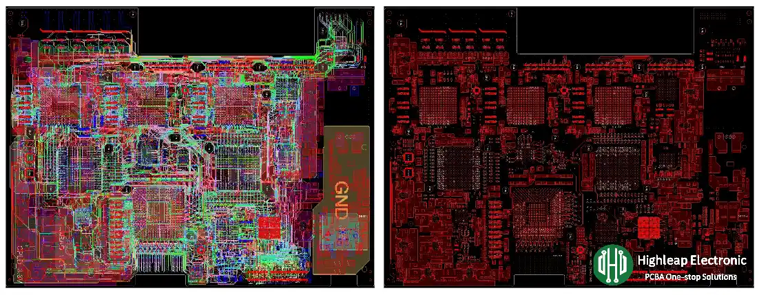
A 28-layer PCB design sits at the intersection of maximum routing density and genuine manufacturing complexity. It is chosen when 24 layers cannot absorb the signal layer count required by a complex system, when power delivery demands more dedicated planes than a lower layer count provides, or when the component density of an AI processor, network switch ASIC, or advanced FPGA demands a board that can route every signal at controlled impedance. This guide is written for design engineers and procurement managers working on real 28-layer programs — it covers the decisions that determine whether a 28 layer PCB manufacturer can actually build your design to specification.
1. When Is 28 Layers the Right Layer Count?
1.1 Routing Density Requirements That Drive 28-Layer Decisions
The decision to use 28 layers is rarely made arbitrarily. It typically follows a structured layer count analysis: a routing density estimate (total net length divided by available routing area per layer) that demonstrates 24 layers cannot accommodate the signal count at the required trace width and spacing. Common triggers:
- BGA packages above 2,500 pins with 0.8 mm or 1.0 mm pitch, where escape routing requires multiple signal layers per package side
- Multi-chip packages (MCM or 2.5D interposer configurations) where the aggregate I/O count exceeds 24-layer routing capacity
- High-speed serial link counts above 64 differential pairs at 28 Gbps+, where each pair must be routed with reference planes above and below throughout its full length
- Power domains that exceed 6–8 in complexity, requiring dedicated planes for multiple voltage rails to avoid shared-plane noise coupling
If your design does not meet at least two of these criteria, a structured review of 24-layer alternatives is worth completing before committing to 28-layer tooling and manufacturing cost.
1.2 The 28-Layer Advantage Over 24 and 32 Layers
Twenty-eight layers provides four additional routing or plane layers over a 24-layer stackup while remaining in the sequential lamination range that a broader supplier pool can manage (typically 2–3 lamination cycles versus the 3–4 required for 30+ layers). Compared to 32 layers, 28 layers offers meaningfully lower material cost (fewer prepreg and core layers), shorter sequential lamination time, and higher manufacturing yield — while meeting the requirements of the vast majority of 400G networking, AI inference, and advanced FPGA platform designs. Understanding the full PCB fabrication workflow behind sequential lamination helps set realistic lead time and cost expectations before issuing an RFQ.
2. Stackup Planning for 28-Layer High-Speed Designs
2.1 Layer Assignment Principles
A well-planned 28-layer stackup follows established signal integrity principles that become more critical, not less, as layer count increases:
- Every high-speed signal layer must have a continuous reference plane immediately adjacent. At 28 layers, there is no shortage of plane layers — use them to create stripline environments for every critical signal group. Microstrip routing on outer layers should be reserved for signals where the controlled-impedance requirement is secondary.
- Maintain symmetry about the board mid-plane. An asymmetric stackup — different copper weights, different dielectric thicknesses, or different numbers of signal and plane layers on each side of the center — creates a net bending moment across the board during lamination and thermal cycling. At 28 layers and 3.0–3.6 mm finished thickness, warpage from asymmetric stackups is difficult to correct and may cause assembly failures. IPC Class 3 requires bow and twist ≤0.5%.
- Group power planes by voltage domain, with signal layers between them where possible. A plane pair (power + ground) between two signal layers functions as a decoupling capacitor with very short loop inductance — a genuine PDN advantage. Design the stackup so this geometry is used for the noisiest power domains.
For ultra-fine-pitch BGA escape routing at 28 layers, HDI via structures — stacked microvias and via-in-pad — are frequently required. These demand a manufacturer with an active sequential lamination line and dedicated laser drilling capability, not just the ability to quote the layer count.
2.2 Dielectric Thickness and Impedance Targets
At 28 layers, dielectric thicknesses between signal layers and their reference planes are typically in the 75–150 µm range for inner stripline layers. This drives trace widths — a 50 Ω single-ended trace over a 100 µm dielectric with Er = 3.7 (Isola 370HR) is approximately 170–180 µm wide, which is manageable for modern impedance-controlled PCB manufacturing. For 100 Ω differential pairs, the trace width and spacing combination must be characterized by the manufacturer’s field solver using actual stackup geometry — not approximated from online calculators.
Thinner dielectrics (75 µm or less) enable tighter coupling between differential pairs and lower parasitic capacitance on high-speed nodes, but require a manufacturer with demonstrated capability to hold dielectric thickness tolerance (±10% of nominal after lamination is the IPC Class 3 requirement). At 75 µm nominal, ±10% means ±7.5 µm — a tolerance that requires the manufacturer to characterize prepreg resin flow precisely for each material combination and lamination recipe.
3. Signal Integrity at 28 Gbps and Above
3.1 Insertion Loss Budget for 28-Layer Boards
Achieving the high-frequency signal performance that 28 Gbps+ serdes links demand requires careful material selection and copper foil specification before the stackup is frozen. A 28 Gbps NRZ signal (14 GHz fundamental) crossing a 300 mm board on an inner stripline layer encounters conductor loss, dielectric loss, and via losses. In a typical 28-layer board using Isola 370HR with standard copper:
- Conductor loss (standard ED copper): approximately 0.18–0.22 dB/cm at 14 GHz
- Dielectric loss (Df = 0.021 at 10 GHz): approximately 0.12–0.15 dB/cm at 14 GHz
- Combined channel loss for 300 mm: 9–11 dB, before via contributions
This budget is marginal for 28 Gbps NRZ without equalization. For designs that require lower loss — or for PAM4 signaling at 56 Gbps (28 Gbaud) where the loss budget is tighter — Panasonic Megtron 6 (Df = 0.002) with VLP copper reduces the combined loss to approximately 5–6 dB for the same channel length, providing substantial margin for equalization and system reliability.
The practical implication: the material choice for a 28-layer design at 28 Gbps+ is not a secondary decision. It should be made early in the design process, driven by measured channel loss budget from a pre-layout simulation, and locked before the manufacturer is selected — because not all 28-layer manufacturers stock or regularly process Megtron 6.
3.2 Via Discontinuity and Back-Drilling at 28 Layers
A through-via in a 28-layer board that is only used for a fraction of the board thickness leaves a stub that resonates within the signal bandwidth. For a 28-layer board with 3.2 mm finished thickness where a via connects only layers 1–14, the unused stub is approximately 1.6 mm — resonating at approximately 30 GHz. For 28 Gbps NRZ signals with energy to 14 GHz, this resonance is at the harmonic boundary; for 56 Gbps signals, it is directly in-band.
Back-drilling removes the unused via stub, leaving a controlled remnant typically ≤0.25 mm. The process requires depth-controlled mechanical drilling with ±50–75 µm Z-axis accuracy and a dimensional compensation model calibrated to each board thickness. Request cross-section photographs of back-drilled vias from the manufacturer’s recent production — measured stub remnant length is directly visible in section and is the most reliable verification of their back-drill process capability.
4. Power Delivery Network Architecture in 28-Layer Boards
4.1 Plane Count and Power Domain Isolation
A 28-layer design typically allocates 10–14 layers to planes (power and ground combined) and 14–18 layers to signal routing. This plane density enables genuine power domain isolation: separate dedicated planes for core voltage, I/O voltage, analog supply, DDR termination voltage, and auxiliary rails — each with its own return path and decoupling strategy. The alternative — shared planes with split copper pours — introduces high-frequency coupling between power domains that is difficult to model and difficult to eliminate in an existing layout.
For AI data center boards and high-end networking platforms where tens of amperes at sub-1V core voltage must be delivered with millivolt-level ripple, the PDN design is co-designed with the stackup. The plane pairs chosen for core voltage must be identified before placement begins, not assigned to whatever layers are left after signal routing is complete.
4.2 Decoupling Capacitor Placement and Via Stub Effects
Decoupling capacitors placed on the board surface must connect to the power and ground planes through via structures. Each via introduces inductance — approximately 0.5–1.0 nH for a standard via through a 3.2 mm board. At 28 layers where power planes may be deep in the stackup, the via inductance from a surface-mounted decoupling capacitor to the relevant power plane may be significant enough to reduce the capacitor’s effectiveness above 100–200 MHz. Minimizing this via inductance requires using via arrays (multiple vias in parallel) and placing decoupling capacitors on the layer closest to the component they serve — which at 28 layers often means embedding them in the stackup at an intermediate lamination stage.

5. Translating SI Requirements into Fabrication Specifications
5.1 The Specification Elements That Must Be Explicit
A panelized 28-layer PCB order that specifies only the Gerber data and a layer count is not a fabrication specification. The following elements must be explicitly stated in writing:
- Laminate material by manufacturer, grade, and IPC-4101 slash sheet designation (e.g., “Isola 370HR, /126”)
- Copper foil type and weight by layer or layer group (e.g., “VLP copper, 0.5 oz on inner signal layers L3–L26”)
- Controlled impedance targets with net class, layer assignment, and tolerance (e.g., “100 Ω differential, L5/L6 pair, ±5%”)
- Back-drill requirements: which via groups, drill direction, maximum stub length
- IPC class: explicitly “IPC-6012 Class 3” — do not leave this unstated
- Surface finish with thickness specification (e.g., “ENIG, 2 µin Au minimum / 150 µin Ni”)
- Test requirements: 100% flying probe or fixture electrical test, TDR impedance coupon test per panel
5.2 DFM Review as a Supplier Qualification Event
Request the manufacturer’s DFM review output before approving production. A capable 28-layer manufacturer will flag real issues: annular ring violations at high-aspect-ratio vias, back-drill clearance conflicts, copper balance problems that predict warpage, or prepreg selection issues at thin dielectric targets. A manufacturer that returns DFM review with no comments on a complex 28-layer design has either not reviewed the files or does not have engineers capable of reviewing them. Both outcomes should disqualify the supplier.
6. Evaluating a 28-Layer PCB Supplier: The Evidence That Matters
6.1 The Supplier Evidence Matrix
| Capability Claim | Evidence to Request | What It Proves |
|---|---|---|
| Sequential lamination to 28+ layers | Cross-section images from active 28L production in last 90 days | Process is current and actively controlled |
| ±5% impedance control | TDR coupon data with Cpk ≥1.33 from ≥5 production panels | Capability is statistical, not one-time |
| IPC Class 3 via plating | Cross-section from via with aspect ratio ≥10:1, with barrel copper measurements | Plating chemistry (PPR) adequate for deep vias |
| Back-drilling | Cross-section showing stub remnant ≤0.25 mm from recent production | Depth control calibrated and verified |
6.2 Red Flags During Supplier Evaluation
- The supplier cannot produce cross-section images from 28-layer production in the past 90 days — indicates 28L is not active production for them
- Impedance Cpk data is unavailable or shows Cpk <1.33 — indicates inadequate process control for ±5% tolerance
- The supplier does not use a field solver (Polar SI, iCD, or equivalent) for impedance calculation — indicates trace widths are estimated, not modeled
- DFM review turnaround is under 4 hours for a complex 28-layer design — indicates the files were not reviewed by an engineer
- The supplier cannot name the plating chemistry used for high-aspect-ratio vias — indicates unfamiliarity with Class 3 plating requirements
Discuss Your 28-Layer PCB Project
7. Lead Time, Cost Drivers, and Prototype-to-Production Transition
7.1 Realistic Lead Time for 28-Layer PCB Prototypes
A 28-layer prototype at a qualified manufacturer takes 15–25 business days from DFM approval to delivery. The lead time is dominated by the sequential lamination schedule (each cycle requires press time, cure time, and dimensional characterization before the next cycle begins) and the plating sequence (PPR plating for high-aspect-ratio vias requires extended bath time compared to DC plating). Any supplier claiming 28-layer prototype delivery in 5–7 days should be asked specifically how they complete 3 lamination cycles in that timeframe — the physics does not support it.
For production lots of 50–500 boards, lead times of 20–30 business days are typical at qualified suppliers, with material availability being the most common variable. A supplier that stocks Isola 370HR and Megtron 6 in standard thicknesses can start production the day DFM is approved; a supplier that orders material per job adds 1–3 weeks to every order.
7.2 Cost Structure of a 28-Layer PCB
The dominant cost drivers in a 28-layer PCB, in order of impact:
- Material cost: 30–40% of total board cost. Megtron 6 costs 4–6× more than Isola 370HR per unit area. This cost differential must be justified by SI analysis, not defaulted to on the assumption that “better material is better.”
- Sequential lamination labor and press time: Each lamination cycle adds direct cost and extends lead time. Designs that can be built in 2 cycles instead of 3 are meaningfully cheaper — stackup architecture decisions made early in design affect cost significantly.
- Back-drilling: Adds cost per via group that requires drilling, plus extended cycle time. Back-drilling should be applied selectively — only to via groups where stub resonance falls within the signal bandwidth, not universally to all through-vias.
- Surface finish: ENIG adds minimal cost relative to 28-layer board value. ENEPIG for wire bond applications or gold finger requirements adds more. Specify what is needed, but do not default to the most expensive finish without application justification.
7.3 Managing the Prototype-to-Production Transition
The gap between a successful prototype and repeatable production is where most 28-layer programs encounter problems. The prototype was built with extra engineering attention; the production lot runs in batch mode with standard process flow. To protect production quality:
- Request impedance Cpk data from the pre-production lot — not just from the prototype
- Establish a process lock agreement defining the approved laminate lot source, plating parameters, and lamination profile before production begins
- Specify 100% electrical testing — flying probe or fixture — as a contractual requirement in the purchase specification, not a request left to the manufacturer’s discretion
- Align PCB assembly requirements with fabrication tolerances early: surface finish choice, via fill specification, and board flatness directly affect downstream SMT yield, and these parameters should be confirmed between fabrication and assembly teams before the first production lot is released
- Define corrective action procedures in the quality agreement before the first production lot — not after the first failure

Recommended Posts
Rogers TMM3 PCB Manufacturer for Mechanical RF Modules
TMM3 is selected when an RF circuit must behave as part of...

Rogers RO3003 PCB Manufacturer for Automotive Radar and mmWave Modules
A 77 GHz radar board is purchased as a working sensor...

Rogers RO4835T PCB Manufacturer for Thin-Core RF Multilayer Boards
RO4835T is useful when the RF layer must move inside the...
Rogers RO4003C PCB Manufacturer for RF and Hybrid Multilayer Boards
RO4003C is often the point where an RF project stops...
How to get a quote for PCBs
Let us run DFM/DFA analysis for you and get back to you with a report.
You can upload your files securely through our website.
We require the following information in order to give you a quote:
-
- Gerber, ODB++, or .pcb, spec.
- BOM list if you require assembly
- Quantity
- Turn time