
Capacitive Keyboard PCB Manufacturer | Touch Sensor PCBA
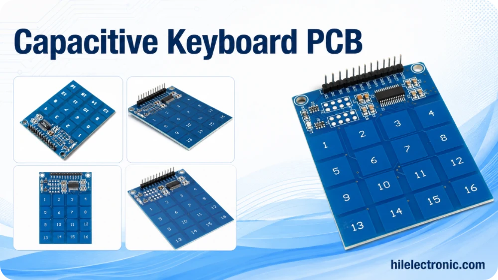
A capacitive keyboard PCB manufacturer must control the electrode, sensor routing, touch controller, grounding, overlay and calibration as one sensing system. A board can pass ordinary electrical inspection and still produce false touches, missed keys or channel-to-channel variation after the final plastic, glass or sealed front panel is installed.
Highleap Electronics supports capacitive keypad and touch sensor PCB fabrication, SMT assembly, controller programming, calibration and functional testing for industrial controls, appliances, access panels and other equipment interfaces. The engineering focus differs from a mechanical keyboard: performance depends on electric-field geometry, noise margin and the completed overlay stack.
Start a Capacitive Keyboard PCB Quote
Share the application, key count or touch area, overlay material and thickness if known, estimated quantity and whether you need bare PCB or complete PCBA. A sketch, photo, sample, Gerber or controller reference can be provided when available. No finished schematic or calibration package is required for the initial quotation.
Capacitive Touch Architecture and Product Requirements
Capacitive keys detect a change in electric field when a finger or conductive object approaches an electrode. Self-capacitance and mutual-capacitance designs use different channel, routing and firmware strategies. The correct architecture depends on key count, overlay, moisture exposure, glove use, proximity requirements and controller capability.
| Architecture | Typical use | Key production concern |
|---|---|---|
| Self-capacitance keys | Discrete buttons and simple keypads | Sensitivity to ground, moisture and channel-to-channel variation. |
| Mutual-capacitance matrix | Higher key count or structured arrays | Transmit/receive routing, coupling and controller tuning. |
| Capacitive slider/wheel | Appliance or control interface | Electrode segmentation and linear response calibration. |
Requirements that should be defined before layout
- Number, size and spacing of keys, sliders or wheels.
- Overlay material, nominal thickness, adhesive and tolerance.
- Bare-finger, glove or proximity operation.
- Expected water film, condensation, cleaning agent or contamination exposure.
- Backlight, display, USB, motor or switching-power noise sources.
- Response time, multi-touch behavior, wake function and power budget.
A sealed front panel may improve cleanability and ingress protection, but the PCB alone does not create an IP rating. The enclosure, gasket, overlay bonding and cable entry must be validated as the complete product. For equipment panels that combine touch with mechanical inputs or displays, the supply route may overlap with custom keypad PCB assembly.
Electrode Geometry, Sensor Routing and Overlay Stack
Electrode area, shape, spacing, hatch pattern and distance to ground determine baseline capacitance and touch delta. Larger electrodes can improve coupling through a thicker overlay but may increase parasitic capacitance or channel interaction. The controller supplier’s design guidance should be reconciled with the final enclosure and graphic-overlay requirements.
Routing and shielding controls
- Keep high-impedance sensor traces short and away from LED, clock, USB and switching-power nodes.
- Use consistent routing among channels so sensitivity differences are intentional rather than accidental.
- Avoid unnecessary vias, large test pads and connectors that add uncontrolled capacitance.
- Define guard or shield nets and whether they are grounded, driven or actively shielded.
- Control copper, solder mask, coating and metal hardware near the electrode area.
| Stack variable | Possible effect | Control |
|---|---|---|
| Overlay thickness/material | Changes touch signal and required threshold | Use released material and tolerance during calibration. |
| Adhesive or air gap | Creates unit-to-unit sensitivity variation | Define lamination method and inspection. |
| Water or contamination | False touches or reduced delta | Use controller features, guard design and product-level environmental test. |
| Backlight/LED switching | Noise coupled into sensor channels | Separate routing/power and test worst-case lighting states. |
Ground shielding is not automatically beneficial. A nearby solid plane can reduce interference but may also reduce touch signal. The optimum stack depends on electrode size, overlay dielectric, enclosure ground and controller architecture. The production drawing should identify areas where copper, labels, adhesive, fasteners or coating are restricted.
Calibration should use the released overlay and mechanical stack. A board tuned in open air should not be treated as production-ready because the final overlay, adhesive and air gaps can shift both baseline and touch margin.
Noise, Moisture, Gloves and False-Touch Control
False touches and missed touches are usually margin problems rather than a single defective component. Power noise, ground changes, moisture, overlay variation, contamination, LED switching and nearby cables can change the sensor baseline or increase noise. The design should maintain a measurable separation between untouched and touched states across the required environment.
Common disturbance mechanisms
| Disturbance | Possible symptom | Design or validation control |
|---|---|---|
| LED or converter switching | Periodic false keys or unstable baseline. | Separate routing and power returns; test at maximum lighting/load states. |
| Water film or condensation | Multiple keys trigger or sensitivity falls. | Use controller moisture features, guard design and product-level wet testing. |
| Thick gloves | Touch delta becomes too small. | Define glove type and tune electrode/thresholds with the approved overlay. |
| Grounded metal or cable changes | Sensitivity changes after installation. | Validate the final enclosure, grounding and cable configuration. |
| Material or coating substitution | Channel thresholds no longer match production. | Treat dielectric changes as calibration-affecting engineering changes. |
Firmware may use baseline tracking, debounce, drift compensation, adjacent-key rejection and moisture modes, but these features require controlled limits. Aggressive filtering can hide noise while making the interface slow or insensitive. Acceptance should therefore include response time and touch margin, not only a pass/fail key event.
Where the interface is used in an industrial environment, protection, traceability and enclosure validation should be coordinated with the requirements described for an industrial keyboard PCB.
PCB Assembly, Programming and Calibration
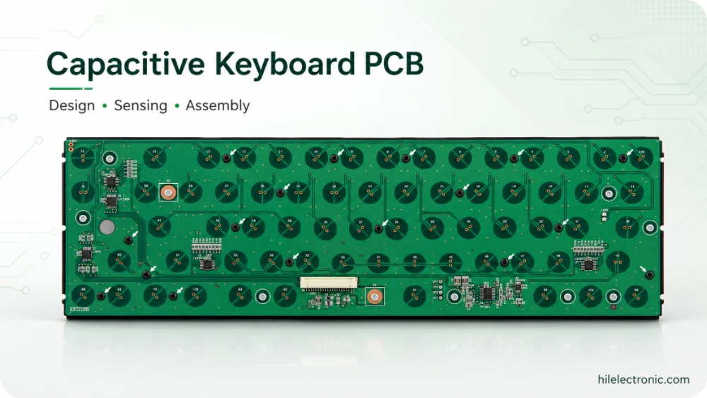
Capacitive PCB production combines ordinary PCBA controls with sensing-specific process control. Electrode geometry, solder mask, coating, adhesive and overlay assembly can all influence capacitance, so changes that would be cosmetic on another board may affect functional performance here.
- Review the electrode design, overlay stack, controller reference design and environmental requirements.
- Fabricate the PCB with controlled outline, copper, solder mask and finish in sensing areas.
- Assemble the touch controller, MCU, power, LEDs, connectors and supporting components.
- Inspect soldering and verify rails, clocks and communication before touch tuning.
- Program the approved firmware, configuration and product identity.
- Install or simulate the released overlay and enclosure stack.
- Measure baseline, noise and touch delta for every channel.
- Apply or verify thresholds and calibration values using the approved procedure.
- Run complete functional and environmental-condition tests before release.
Calibration data and traceability
Calibration may use one common parameter set, channel-specific values or per-unit data depending on product variation and controller capability. The production work instruction should define what is programmed, what is measured and what limits cause rejection. Firmware checksum, calibration revision and test result can be linked to a lot or serial number when required.
Conformal coating, potting or adhesive changes should not be introduced without review. These materials alter dielectric spacing and can reduce sensitivity or require new thresholds. The underlying SMT and inspection controls can be managed through Highleap’s PCB assembly service, but touch calibration remains a product-specific operation.
Functional Validation, Applications and Volume Release
Production validation should measure more than whether a key toggles. Useful parameters include untouched baseline, touch delta, noise amplitude, threshold margin, channel consistency, response time, release behavior and recovery after a disturbance. Testing should use the released firmware and the final or representative overlay stack.
Recommended test conditions
- All keys, sliders or wheels under normal operation.
- Maximum backlight, display, USB and switching-load states.
- Specified temperature and humidity range.
- Defined glove, water-film or cleaning-agent conditions.
- Power cycling, wake-up and baseline-recovery behavior.
- Final enclosure, cable and grounding configuration.
A golden unit or approved data range is useful when touch feel and environmental behavior are product-specific. Repeat orders should use the same test firmware, overlay condition and limits so process drift can be detected rather than normalized.
Applications and production planning
Typical projects include wipe-clean medical or laboratory interfaces, industrial touch controls, appliance keypads, access panels, elevators, kiosks and consumer control surfaces. Application labels do not establish regulatory, medical or ingress compliance; the product owner must define the applicable standards and complete product-level validation.
For the initial quote, the application, key count, dimensions, quantity and required scope are sufficient. Engineering release later adds PCB files, BOM, controller data, overlay drawing, firmware and acceptance limits. Volume supply benefits from controlled PCB material, overlay lots, touch-controller sourcing and formal change review because seemingly equivalent substitutions can alter dielectric or noise behavior.
Projects that combine touch sensing with broader keyboard electronics can also be coordinated through Highleap’s keyboard PCB manufacturing service.
Capacitive Keyboard PCB FAQ
Can capacitive keys work through glass or plastic?
Yes, when electrode geometry, material, thickness, adhesive, air gaps and controller thresholds are designed for that exact overlay stack.
Can a capacitive keypad be waterproof?
It can operate behind a sealed overlay, but waterproof performance belongs to the complete enclosure and must be validated to the required test method.
How is sensitivity calibrated in production?
The released overlay is installed or simulated, then baseline, touch delta, noise and threshold margin are measured for every channel using approved firmware and limits.
Does conformal coating affect touch performance?
It can. Coating changes dielectric spacing and may alter baseline or sensitivity. Material, thickness and keepout areas should be controlled and may require recalibration.
What usually causes false touches?
Common causes include power or LED noise, moisture, grounding changes, overlay variation, contamination, unstable supply rails and thresholds with inadequate margin.
Discuss a Capacitive Keyboard PCB Project
Provide the application, touch-key count or area, overlay information if available, expected quantity and required PCB, PCBA, programming or calibration scope.

Recommended Posts

TMM4 Filter PCB Manufacturing
TMM4 filter PCB manufacturing is controlled by the...

TMM3 PCB Manufacturing for RF Modules
TMM3 PCB manufacturing is most useful where the RF module...

TMM6 PCB Fabrication
TMM6 fabrication is the process-control page for a mid-Dk...

TMM10 PCB Manufacturing for Compact RF Designs
Table of contentsHow TMM10 Shrinks RF StructuresTMM10 vs...
How to get a quote for PCBs
Let’s run DFM/DFA analysis for you and get back to you with a report. You can upload your files securely through our website. We require the following information in order to give you a quote:
-
- Gerber, ODB++, or .pcb, spec.
- BOM list if you require assembly
- Quantity
- Turn time
For PCBA services, please provide your BOM (Bill of Materials) and any specific assembly instructions. We also offer DFM/DFA analysis to optimize your designs for manufacturability and assembly, ensuring a smooth production process.