
Hot Swap Keyboard PCB Manufacturer | Socket Assembly & Testing
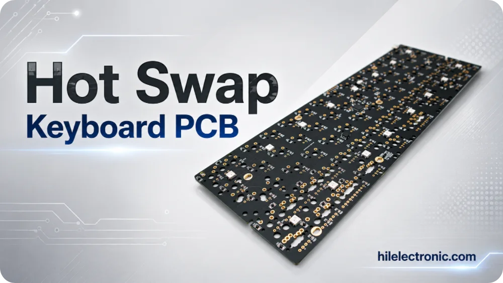
A hot swap keyboard PCB manufacturer must control the socket as both an electrical contact and a mechanically loaded component. Repeated switch insertion transfers force through the socket, solder joints, copper pads, PCB and plate. The exact socket part number, land pattern, stencil aperture, switch-pin path and enclosure support therefore matter more than a generic “hot-swappable” label.
Highleap Electronics manufactures bare boards and assembled hot-swap keyboard PCBAs with matrix diodes, per-key RGB lighting, controllers, USB-C interfaces, encoders and displays. Scope can include socket sourcing, SMT/THT assembly, firmware programming, full-key tests and pilot mechanical-fit checks.
Start a Hot Swap Keyboard PCB Quote
Share the keyboard layout, socket type or reference if known, required quantity and whether you need bare PCB, socket assembly or a complete PCBA. Gerber, BOM, plate drawings, photos or a sample board are useful when available, but no schematic is required for the initial quotation.
Hot-Swap Socket Architecture and Compatibility
A hot-swap board replaces soldered switch leads with contacts mounted on or inserted into the PCB. The keyboard matrix still uses rows, columns and usually one diode per switch, but the socket adds another contact interface and another mechanically stressed solder joint. The electrical design should therefore be reviewed together with the keyboard matrix and diode map.
SMT sockets and through-hole receptacles are different systems
| Socket solution | Typical assembly route | Compatibility control |
|---|---|---|
| Kailh-style hot-swap socket | Bottom-side SMT reflow | Approve exact MPN, land pattern, orientation, switch family and plate stack. |
| Gateron-style hot-swap socket | Bottom-side SMT reflow | Do not assume drop-in equivalence; verify supplier drawing and pilot insertion. |
| Mill-Max-style receptacle | Individual plated through-hole insertion and soldering | Verify receptacle series, PCB hole size, switch-pin fit, seating height and solder process. |
Brand names are not sufficient release data. Socket housings that appear similar can differ in pin-entry geometry, orientation marks, recommended land pattern and reflow limits. The approved BOM should identify the exact manufacturer part number, and the pilot build should use the intended switches, plate and PCB thickness.
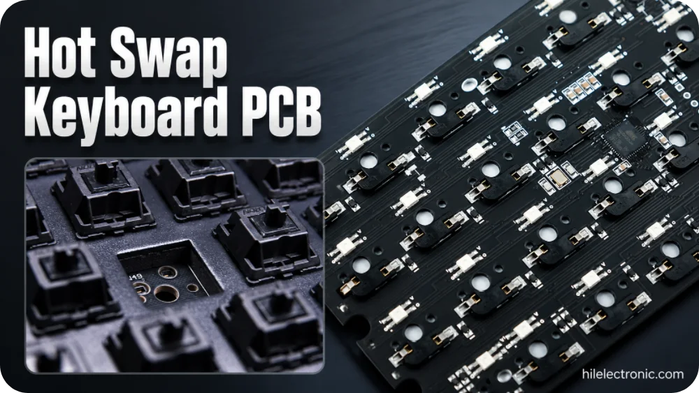
Many hot-swap keyboards use a two-layer PCB with sockets on the bottom side. LEDs, diodes, MCU and USB components may be fitted on one or both sides. Copper-layer count and assembly-side count should be stated separately because they affect routing, stencil design, reflow sequence and inspection access.
Footprint, Plate and Mechanical Support Requirements
The socket footprint is only one part of compatibility. The switch center, plate cutout, PCB-to-plate spacing, enclosure standoffs, foam and bottom clearance must form one mechanical stack. A correctly soldered socket can still fail when the switch pin enters off-axis or the PCB bends during insertion.
Release data that should be checked together
- Socket drawing and land pattern: pin-entry location, polarity or orientation, pad size and solder-mask clearance.
- Plate file: switch-center accuracy, cutout tolerance and support around large keys.
- PCB thickness and support: board flex between standoffs, especially near spacebar and edge keys.
- Bottom-side clearance: socket housing, solder fillets, LEDs, foam and case ribs must not interfere.
- Switch sample: the production switch family should be used for insertion and fit approval.
Universal layouts require additional control. ANSI/ISO options, split backspace, split spacebar and multiple bottom rows can place sockets close together or create overlapping mechanical keepouts. Each sellable variant should have a controlled assembly drawing and test map rather than relying on one generic PCB image.
Where the design uses angled switch groups, the plate and enclosure review becomes more important. The same socket process can be applied to an Alice keyboard PCB, but rotated switch positions and nonstandard stabilizers increase the risk of off-axis insertion.
Hot-Swap PCB Assembly and Inspection Process
Hot-swap sockets are repetitive SMT components, but their mechanical function makes paste volume, seating and pad condition critical. A stable production route normally includes the following controls:
- Review the released socket MPN, footprint, stencil aperture, plate and enclosure stack.
- Fabricate and electrically test the bare PCB, including pad geometry, holes and board outline.
- Inspect incoming sockets and switches for housing damage, bent contacts and lot consistency.
- Verify solder-paste deposition and socket orientation on the first article.
- Place and reflow sockets with the approved profile and board support.
- Use AOI plus focused side-view inspection where the joint is partly hidden by the housing.
- Assemble diodes, LEDs, controller, USB connector and other SMT/THT parts.
- Program firmware and run socket insertion sampling and full-key functional testing.
Inspection method should match the actual risk
X-ray is not automatically required for every socket. AOI, side-view microscopy, first-article solder evaluation, controlled insertion tests or pull/shear studies may provide more relevant evidence depending on joint visibility and customer acceptance criteria. Rework instructions should define heating method, maximum cycles and pad-repair criteria because removing a mechanically anchored socket can easily damage copper pads.
For a complete PCBA, socket inspection should be integrated into the wider PCB assembly process, including component traceability, first-article approval and firmware revision control.
Reliability Risks, Full-Key and Insertion Testing
Hot-swap failures are often incorrectly treated as simple solder defects. The root cause may be the switch pin, plate alignment, unsupported PCB, contaminated contact, matrix diode or firmware map. Failure analysis should separate these mechanisms before rework.
| Problem | Likely causes | Corrective controls |
|---|---|---|
| Socket moves or becomes loose | Insufficient solder, poor wetting, weak pad geometry, repeated off-axis insertion | Revise stencil/land pattern, verify finish and paste, improve PCB support and plate alignment. |
| Switch pin misses the contact | Wrong footprint, bent pin, misaligned plate or socket orientation | Use approved samples, mechanical stack review and guided insertion check. |
| Intermittent key | Contaminated contact, damaged spring, cracked solder joint or matrix fault | Separate socket contact test from diode/matrix continuity and inspect under mechanical load. |
| Lifted PCB pad during rework | Excess heat, repeated cycles or pulling socket before solder is molten | Use controlled rework tooling, temperature profile and pad-repair criteria. |
| Switch difficult to remove | Plate tolerance, housing interference or unsupported PCB flex | Check plate cutout, enclosure standoffs and removal-force method. |
Production test coverage
A useful end-of-line plan verifies every physical key position and records the failing coordinate. It should also cover diode direction, USB enumeration, RGB mapping, encoders, displays and bootloader access when fitted. Claims such as 6KRO or NKRO must be confirmed with the released firmware and defined key combinations; per-key diodes alone do not prove the final rollover behavior.
- Actuate every socket with a controlled switch or dedicated probe.
- Sample insertion and removal without visible socket movement or PCB flex damage.
- Test USB operation in both cable orientations when USB-C is used.
- Run defined RGB patterns and compare physical LED positions with firmware indices.
- Use a golden unit for plate fit, switch feel and enclosure-clearance comparison.
- Record defects by socket, key coordinate and failure category to support corrective action.
Where the product has a complex feature set, a dedicated functional test fixture is more reliable than manual typing because it produces repeatable coverage and traceable results.
Customization, Project Inputs and Volume Supply
Hot-swap PCB projects include gaming keyboards, compact custom keyboards, macropads, ortholinear boards and ergonomic layouts. Customization may include ANSI/ISO variants, socket brand, switch orientation, per-key RGB, underglow, encoders, displays, solder-mask color, branding, firmware and packaging.
Information needed at each project stage
| Project stage | Useful input | Primary output |
|---|---|---|
| Initial quotation | Layout, socket preference, quantity and supply scope. | Feasibility questions and preliminary manufacturing route. |
| Engineering release | Gerber, BOM, centroid, plate/enclosure files and firmware. | DFM, stencil, fixture and first-article plan. |
| Pilot build | Approved switches, keycaps, plate and golden-unit criteria. | Mechanical fit, socket process and full-function approval. |
| Volume production | Frozen revisions, forecast, packaging and traceability needs. | Repeatable PCBA supply and controlled change management. |
Unit cost is influenced by socket quantity and MPN, board size, assembly sides, RGB count, controller complexity, test time, panel utilization and order volume. Stable socket and MCU sourcing, controlled variants and fixture reuse generally matter more than reducing a single PCB specification. The broader service can be coordinated through Highleap’s keyboard PCB manufacturing capability.
Hot Swap Keyboard PCB FAQ
Are common Kailh- and Gateron-style sockets SMT or through-hole?
Common bottom-mounted hot-swap sockets are SMT parts. Mill-Max-style receptacles are separate through-hole contacts and use different hole, seating and soldering requirements.
Can one footprint accept multiple socket brands?
Only after the exact part drawings and physical samples have been validated. Similar brand descriptions do not guarantee the same housing, pad or switch-pin geometry.
How can loose sockets be prevented?
Use the approved land pattern and stencil, control solder wetting and seating, align the plate, support the PCB and perform insertion sampling under the intended mechanical stack.
Does a hot-swap keyboard automatically support NKRO?
No. Rollover depends on matrix diodes, firmware scanning, HID report format and the tested key combinations. Socket type does not determine NKRO.
Can the initial quote start without complete production files?
Yes. A layout, socket reference, quantity and required supply scope are sufficient for the first review. Detailed files are confirmed before engineering release.
Discuss a Hot Swap Keyboard PCB Project
Provide the layout, socket preference, approximate quantity and whether you need bare PCB, socket assembly or a fully programmed PCBA.

Recommended Posts

TMM4 Filter PCB Manufacturing
TMM4 filter PCB manufacturing is controlled by the...

TMM3 PCB Manufacturing for RF Modules
TMM3 PCB manufacturing is most useful where the RF module...

TMM6 PCB Fabrication
TMM6 fabrication is the process-control page for a mid-Dk...

TMM10i PCB Fabrication and DFM
TMM10i PCB fabrication has a stronger DFM emphasis because...
How to get a quote for PCBs
Let’s run DFM/DFA analysis for you and get back to you with a report. You can upload your files securely through our website. We require the following information in order to give you a quote:
-
- Gerber, ODB++, or .pcb, spec.
- BOM list if you require assembly
- Quantity
- Turn time
For PCBA services, please provide your BOM (Bill of Materials) and any specific assembly instructions. We also offer DFM/DFA analysis to optimize your designs for manufacturability and assembly, ensuring a smooth production process.