Back to blog
What is Electrical Impedance and its role in PCB
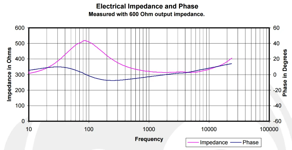
Electrical lmpedance and PhaseMeasured with 600 Ohm output impedance
Electrical impedance is fundamental in the behavior of electrical devices and circuits, playing a crucial role in physics and electrical engineering. Impedance represents the resistance a circuit offers to alternating current (AC), much like an audio signal. In purely resistive circuits, impedance is synonymous with resistance. However, impedance offers a more comprehensive understanding of how circuits resist the flow of current, especially when reactive components like capacitors and inductors come into play.
This article offers a deep dive into the nuances of electrical impedance, highlighting its importance in PCB design and detailing the factors influencing impedance in electrical circuits.
Fundamental Concepts of Electrical Impedance
Electrical impedance, represented symbolically as 𝑍, is the total opposition a circuit offers to the flow of alternating current. It is a vector quantity comprising both magnitude and phase and is measured in ohms (Ω). The equation governing impedance in its most basic form is:
Z=V/I
where 𝑉 is the voltage across the component, and 𝐼 is the current flowing through it.
Unlike resistance, which only impedes direct current (DC), impedance extends the concept by incorporating the effects of capacitance and inductance, which are frequency-dependent. This interaction can be mathematically expressed as:
Z=R+jX
Here, 𝑅 represents the resistive component, and 𝑗𝑋 denotes the reactive component, where 𝑗 is the imaginary unit.
Detailed Analysis of Impedance Components
1.Resistive Component (R): Resistance occurs due to the inherent opposition within the conductors to the flow of electrons. It results in the dissipation of energy in the form of heat and does not vary with frequency.
2.Reactive Component (X): This component is split into:
- Inductive Reactance (XL ): Arising from inductors in a circuit, it is directly proportional to the frequency and is given by 𝑋L=2𝜋𝑓𝐿, where 𝑓 is the frequency, and 𝐿 is the inductance.
- Capacitive Reactance (Xc): Generated by capacitors, this reactance is inversely proportional to the frequency, formulated as Xc =1/(2πfC), with C representing capacitance.
The overall impedance can therefore be influenced by changing the frequency of the input signal, a property utilized in various electronic applications, such as tuning radio frequencies and impedance matching in audio systems.
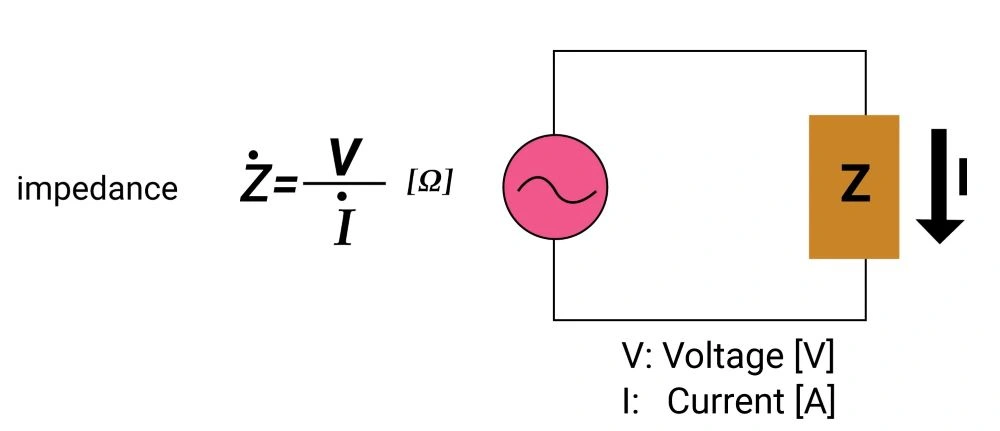
Electrical impedance calculation formula
Applications of Electrical Impedance
Impedance finds extensive applications in various electrical and electronic systems:
- Audio Systems: Ensuring proper impedance matching between audio sources and speakers is crucial for sound quality.
- Power Systems: Impedance impacts power distribution by influencing signal propagation and leakage.
- PCB Design: Impedance control ensures efficient signal transmission and minimizes interference in high-frequency circuits.
This video tutorial provides a basic introduction into impedance. Impedance is the opposition to the flow of AC where as resistance is the opposition to the flow of DC.
Electrical impedance in PCB
In the field of electronics, we often discuss the importance of Electrical Impedance and its application in various circuits and electronic devices. However, today I would like to bring up a closely related topic – PCB Impedance.
We know that Electrical Impedance is a broad concept that involves the performance and stability of the entire circuit system. However, in actual circuit design and manufacturing, PCB serves as the carrying platform of the circuit, and the impact of its impedance characteristics on the entire system cannot be ignored. So, what exactly does PCB Impedance do? Why do we need to pay special attention to impedance issues in PCB design?
Next, I will delve into the related content of PCB Impedance. Through understanding of PCB Impedance, we will better understand how to optimize the design of printed circuit boards and improve the performance and reliability of circuit systems.
The Crucial Role of Impedance Control in PCB Design
In today’s complex electronic field, impedance control plays a key role in PCB design. As high-frequency signals increasingly saturate electronic devices, achieving and maintaining proper impedance matching has become the foundation of excellent PCB design. The reason behind this is simple, that is, impedance mismatch can cause a series of adverse effects, such as signal reflection, attenuation, and crosstalk. Therefore, in order to ensure the integrity, reliability and good performance of electronic systems, it is absolutely necessary to pay high attention to impedance control.
To gain a deeper understanding of the crucial fundamentals of impedance control, it is necessary to explain the basic mechanisms that control signal propagation in PCBs. In essence, impedance represents the resistance of a circuit to the flow of alternating current. In PCB designs, high-frequency signals travel through a variety of complex paths, and maintaining consistent impedance levels is critical to mitigating signal distortion and attenuation. This requires careful consideration of many factors, including trace geometry, dielectric materials, and layer stack-up, so that the impedance of the signal traces matches the impedance of the connecting components and transmission lines.
The consequences of impedance mismatch go beyond signal distortion and permeate every aspect of electronic design and functionality. Signal reflections are one of the common consequences of impedance mismatch, which occurs when part of the signal bounces due to impedance changes along the transmission path. This phenomenon not only damages the integrity of the signal, but also puts additional stress on the electronic components, potentially causing system instability or even failure. Moreover, impedance mismatch can also exacerbate signal attenuation, causing the signal strength to decrease after being transmitted over longer distances, which is particularly harmful in high-speed digital circuits and radio frequency applications. In addition, crosstalk (that is, unwanted signal coupling between adjacent traces) increases significantly in an impedance mismatched environment, further exacerbating signal interference and signal degradation. Therefore, meticulous impedance control has become the key to optimizing the function, reliability and life of modern electronic systems!
Methods for Controlling Impedance in PCB Design
Trace Geometry Optimization
Optimizing trace width, thickness, and spacing ensures that impedance remains consistent across the PCB. Microstrip and stripline designs provide different impedance characteristics, allowing designers to choose the best configuration for their needs.
Material Selection
Selecting PCB materials with the appropriate dielectric properties ensures consistent impedance control. High-frequency circuits often require specialized materials to minimize signal loss.
Simulation and Testing
Simulating impedance using tools like electromagnetic field solvers provides insights into potential issues before physical prototypes are made. Testing with time-domain reflectometry (TDR) verifies impedance control in actual PCBs.
Design Guidelines
Adhering to established design guidelines for trace layout, ground planes, and spacing helps maintain consistent impedance. Industry standards like IPC-2141 offer guidelines for impedance control in PCB design.
Conclusion
In this article, we explore the complexity of electrical impedance and its importance in PCB design. As a PCB engineer, I know the critical role electrical impedance plays in PCB design. Additionally, I cover methods for controlling impedance in PCB design, such as trace geometry optimization, material selection, simulation, and testing. By following these methods and design guidelines, we can ensure efficient signal transmission and minimize interference in high-frequency circuits. I hope you apply these concepts in your future PCB designs and achieve optimal performance.
FQA
1.How does impedance matching impact signal transmission in audio systems?
In audio systems, impedance matching between audio sources and speakers is crucial for optimal sound quality. When the output impedance of a source matches the input impedance of a speaker, maximum power transfer occurs, minimizing signal loss and distortion. This ensures efficient signal transmission and enhances the fidelity of reproduced audio.
2.What role does impedance play in power distribution networks?
Impedance significantly influences power distribution by affecting signal propagation and leakage within the network. High impedance can lead to increased voltage drop and power loss, compromising the efficiency and stability of the distribution system. Thus, minimizing impedance in power distribution networks is essential for maintaining stable voltage levels and ensuring reliable power supply to connected devices.
3.How does impedance control contribute to signal integrity in PCB design?
In PCB design, impedance control is paramount for ensuring reliable signal transmission, particularly in high-frequency circuits. Proper impedance matching minimizes signal reflection, attenuation, and crosstalk, thereby preserving signal integrity and maximizing performance. By meticulously managing impedance through trace geometry optimization, material selection, and simulation/testing, designers can mitigate the adverse effects of impedance mismatch and optimize signal transmission efficiency.
4.What are the key methods and tools for controlling impedance in PCB design?
Controlling impedance in PCB design involves various methodologies and tools. Trace geometry optimization, including adjusting trace width, thickness, and spacing, helps maintain consistent impedance levels across the PCB. Material selection is critical, with specialized dielectric materials chosen to minimize signal loss in high-frequency circuits. Simulation tools like electromagnetic field solvers aid in predicting and analyzing impedance characteristics, while testing methods like time-domain reflectometry (TDR) verify impedance control in actual PCBs. Adhering to industry-standard design guidelines, such as those outlined in IPC-2141, ensures best practices for impedance control in PCB design, ultimately leading to optimized performance and reliability.
5.What are the practical implications of impedance mismatch in electronic circuits, beyond just signal distortion?
Impedance mismatch in electronic circuits can lead to a range of adverse effects beyond signal distortion, including signal reflection, attenuation, and crosstalk. These effects can compromise the integrity, reliability, and performance of electronic systems, potentially leading to instability or failure.
PCB & PCBA quick quote
Related Articles
Comprehensive Guide to Electronic HS Codes for PCBA
Export PCBAIn the realm of international trade, HS Codes (Harmonized System codes) are crucial for the classification and categorization of goods. Developed by the World Customs Organization (WCO), these numerical codes provide a standardized method for customs...

Chinese Chips: A Comprehensive Guide for Tech Enthusiasts
Chinese ChipsIn recent years, China's semiconductor industry has experienced a significant transformation, establishing itself as a major player in the global chip market. With advancements in technology and substantial investments in research and development, Chinese...
What is an Integrated Circuit (IC) and its Types
Integrated Circuit PCBAConceived independently by Jack Kilby and Robert Noyce in the mid-20th century, the integrated circuit marked a significant leap in technology. Kilby’s successful creation of the first functional IC in 1958 propelled semiconductor technology to...
What does .DXF file mean? How to convert to gerber file?
CAD DXF FilesAs a PCB engineer working at the heart of electronic device manufacturing, I’ve seen firsthand the vital role that detailed design files play in our projects. Among these, DXF (Drawing Exchange Format) files are particularly crucial. Originating from the...
Take a Quick Quote
