
15 Years in PCB Engineering – Key Lessons on Design, Safety, and Innovation

PCB Engineering
Navigating the intricate landscape of PCB Engineering requires not only a solid grasp of design fundamentals but also a clear awareness of the pitfalls that can compromise circuit board reliability and manufacturability. This article draws on 15 years of hands-on experience in PCB design and layout optimization, offering practical insights on how to elevate your engineering practice while avoiding common PCB design mistakes.
As a PCB engineer with 15 years of experience, I have witnessed the evolution of the PCB industry in China—from simple single-sided boards to today’s complex multi-layer PCB designs that power advanced electronics. Throughout my career, I have learned that success in PCB Engineering depends heavily on careful planning, design for manufacturability (DFM), and attention to detail in every trace, via, and layer assignment. Here, I share the key lessons and best practices for PCB that continue to guide my approach.
1. Design for Manufacturability (DFM) in PCB Engineering
Key Practices
Component Placement Optimization
In PCB Engineering, strategic component placement is critical to manufacturability and long-term reliability. Proper spacing helps prevent soldering defects and reduces heat concentration. Techniques such as thermal relief pads enable more effective heat dissipation, particularly for high-power or high-density components.
Trace Routing Excellence
Consistent trace widths and spacing are essential to avoid etching anomalies and maintain impedance control. In high-speed PCB design, applying advanced routing strategies—such as differential pair routing and controlled impedance traces—can significantly improve signal integrity and overall board performance.
Common Pitfalls
Disregarding Manufacturer Guidelines
A frequent issue in PCB Engineering is neglecting the specifications set by PCB manufacturers regarding stackup configurations, trace width, hole size, and clearance rules. Ignoring these parameters can result in production delays, yield loss, and higher costs. Effective collaboration with your fabrication partner ensures your design remains manufacturable while meeting both performance and reliability goals.
2. Thermal Management in PCB Engineering
Key Practices
Strategic Heat Dissipation
Effective thermal management in PCB Engineering requires a holistic strategy that leverages thermal vias, heat sinks, and copper pours to dissipate heat from power-dense components. Optimizing thermal pathways is vital to enhance both performance and reliability. Advanced simulation tools such as ANSYS Icepak or FloTHERM support accurate thermal analysis, guiding PCB engineers in judicious component placement and layout refinement for improved heat flow.
Material Selection Expertise
Choosing the right substrate is critical for robust PCB thermal design. High-thermal-conductivity ceramics or premium FR4 laminates with low coefficient of thermal expansion (CTE) can withstand thermal cycling and ensure long-term stability. In PCB Engineering, careful evaluation of material properties and environmental constraints enables engineers to align thermal performance with project requirements.
Common Pitfalls
Underestimating Thermal Considerations
A common mistake in PCB Engineering is overlooking heat management early in the design phase. Insufficient planning can trigger thermal runaway, reducing component lifespan and reliability. By integrating thermal simulation and predictive modeling early in the workflow, PCB engineers can proactively identify thermal bottlenecks and implement cost-effective mitigation strategies before manufacturing begins.

BLDC driver board power supply schematic diagram–PCB Engineering
3. Signal Integrity in PCB Engineering
Key Practices
Rigorous Impedance Control
Successful PCB Engineering requires precise impedance matching across high-speed signal traces to maintain signal integrity. In designs with narrow pulse widths and tight timing margins, even small deviations can lead to data corruption or performance degradation. By leveraging advanced impedance modeling tools such as Polar Si9000e, PCB engineers can validate impedance profiles, optimize differential pair routing, and ensure reliable high-speed signal transmission.
Ground Plane Optimization
Establishing solid ground planes is a cornerstone of signal integrity in PCB Engineering. Properly designed ground planes suppress electromagnetic interference (EMI), minimize ground bounce, and stabilize reference voltages. Incorporating stitching vias at regular intervals reduces loop inductance and improves return path continuity, reinforcing overall system stability and signal quality.
Common Pitfalls
Disregarding Signal Integrity Principles
Inadequate routing practices—such as inconsistent trace widths, poor spacing, or lack of impedance control—can trigger timing violations, crosstalk, and data loss. A disciplined approach to high-speed PCB layout, emphasizing impedance matching, trace-to-trace spacing, and EMI mitigation, is essential for safeguarding signal integrity in modern electronics.
4. Layer Management and Via Utilization in PCB Engineering
Key Practices
Strategic Layer Allocation
In advanced PCB Engineering, multilayer PCB stackups are essential to accommodate complex circuit topologies and improve electromagnetic compatibility (EMC). By segregating high-speed signal layers from sensitive analog or digital domains, engineers can reduce crosstalk and optimize system stability. Using signal integrity simulation tools such as Cadence Sigrity enables early validation of layer stackups and via assignments, ensuring a balanced design for both performance and manufacturability.
Sophisticated Via Selection
Proper via utilization is a cornerstone of high-density PCB Engineering. Through-hole vias are suitable for basic interlayer connectivity, while blind and buried vias are indispensable in high-density interconnect (HDI) designs. Additionally, via stitching techniques can reinforce power distribution networks (PDN), reduce voltage droop, and enhance current-handling capacity in demanding applications.
Common Pitfalls
Excessive Via Proliferation
A common issue in PCB Engineering is the overuse of vias, which can compromise signal integrity, increase inductance, and escalate manufacturing costs. Employing advanced routing strategies that minimize unnecessary vias while preserving critical signal paths ensures both cost efficiency and robust signal performance.

PCB Engineering
5. Testing and Validation in PCB Engineering
Key Practices
Comprehensive Test Coverage
In PCB Engineering, thorough testing is essential to ensure both functionality and long-term reliability. Incorporating well-placed test points throughout the PCB layout facilitates effective debugging and functional validation across digital, analog, and mixed-signal domains. Techniques such as boundary scan (IEEE 1149.1 JTAG) streamline in-circuit testing (ICT), expanding test coverage for complex, high-density PCB assemblies.
Prototype Iteration Discipline
Prototyping is an indispensable step in the PCB design lifecycle. By validating performance, detecting design flaws, and refining manufacturability, prototypes reduce risks before mass production. Rapid prototyping methods—including CNC machining and 3D printing—enable faster iteration cycles, minimize redesign costs, and accelerate time-to-market.
Common Pitfalls
Neglecting Prototype Validation
One of the most critical mistakes in PCB Engineering is skipping prototype validation. Overlooking this step often leads to expensive design revisions, delayed schedules, and reduced product reliability. Investing in comprehensive prototyping and early validation ensures design integrity, manufacturability verification, and smoother transitions into full-scale production.
6. Documentation and Collaboration in PCB Engineering
Key Practices
Meticulous Documentation Regimen
In PCB Engineering, comprehensive documentation is essential for ensuring seamless collaboration and efficient manufacturing. Deliverables such as Gerber files, assembly drawings, and design specifications provide the foundation for accurate PCB fabrication and assembly. Adopting industry-standard formats like IPC-2581 not only enhances interoperability but also reduces data transfer errors, streamlining the entire manufacturing process.
Stakeholder Engagement Excellence
Effective PCB Engineering requires strong communication with fabricators, assemblers, and test engineers throughout the design cycle. Early engagement helps identify manufacturing constraints, refine design choices, and align with project objectives. Leveraging collaborative platforms like Altium 365 or Siemens Teamcenter supports real-time design collaboration, version control, and transparency across cross-functional teams.
Common Pitfalls
Communication Breakdowns
One of the most common challenges in PCB Engineering is poor communication between design teams and manufacturing partners. Misalignment on design intent can lead to costly revisions and production delays. Establishing structured communication channels, conducting regular design reviews, and centralizing documentation on collaborative platforms ensures stakeholder alignment and minimizes misunderstandings.
Critical Considerations in PCB Implementation
As we delve deeper into the world of PCB design, it becomes clear that considerations go beyond technical features and performance metrics. Environmental sustainability, safety protocols, emerging technologies, regulatory compliance, and reliability engineering all play key roles in shaping the modern PCB design landscape. In order for PCB to be better practiced, the following issues also need to be considered:
1. Environmental Considerations in PCB Design
- How can designers integrate environmental sustainability principles into PCB design?
- What are some eco-friendly materials and manufacturing processes for PCBs?
- Strategies for minimizing electronic waste and maximizing recyclability in PCB design.
2. Security and Cybersecurity in PCB Design
- What are the key security threats facing modern PCB designs?
- Best practices for implementing hardware-level security features in PCBs.
- Considerations for protecting sensitive data and preventing unauthorized access through PCBs.
3. Emerging Technologies and Trends in PCB Design
- Exploration of cutting-edge technologies shaping the future of PCB design, such as flexible and stretchable PCBs, additive manufacturing, and embedded components.
- How are trends like Internet of Things (IoT), edge computing, and artificial intelligence influencing PCB design requirements?
- Challenges and opportunities presented by miniaturization and increasing component complexity.
4.Regulatory Compliance and Certification in PCB Design
- Overview of regulatory standards and certifications relevant to PCB design, such as RoHS, REACH, and UL.
- Strategies for ensuring compliance with international regulations and standards throughout the design process.
- Importance of documentation and traceability for meeting regulatory requirements and facilitating product certification.
5. Failure Analysis and Reliability Engineering for PCBs
- Common failure modes in PCBs and techniques for failure analysis.
- How can reliability engineering principles be applied to PCB design to enhance product longevity and performance?
- Case studies illustrating the importance of reliability testing and design validation in preventing field failures and ensuring customer satisfaction.
Conclusion: Lessons Learned in PCB Engineering
Elevating PCB Engineering from a purely technical task to a strategic discipline requires more than just design skills. It demands meticulous planning, rigorous validation, effective documentation, and seamless collaboration across multidisciplinary teams. By integrating these best practices—and remaining vigilant of common pitfalls—engineers can confidently navigate the complexities of modern PCB design, delivering products that achieve superior performance, reliability, and manufacturability.
Reflecting on my 15 years in PCB Engineering, the journey has been one of continuous learning, adaptation, and innovation. By embracing emerging technologies, adhering to industry standards, and fostering strong collaboration with fabricators, assemblers, and stakeholders, my colleagues and I have consistently delivered high-quality PCB solutions that meet the evolving needs of the electronics industry.
Looking forward, I remain committed to pushing the boundaries of PCB Engineering, sharing insights, and contributing to the advancement of electronics design and innovation.
FAQ
1.How crucial is component selection in PCB design, and what factors should engineers consider?
Component selection profoundly influences the performance, reliability, and manufacturability of PCBs. Engineers should evaluate factors such as component specifications, availability, lead times, and compatibility with the overall system architecture. Additionally, considering the long-term availability of components is essential to mitigate supply chain risks and ensure product longevity.
2.How can engineers ensure robust power integrity in PCB designs?
Robust power integrity is vital for stable and reliable operation of electronic systems. Engineers should conduct comprehensive power integrity analysis, including voltage drop, power delivery network (PDN) impedance, and decoupling capacitor placement. Utilizing tools like Keysight PathWave ADS or Cadence Sigrity PowerSI can facilitate accurate analysis and optimization of power distribution networks.
3.What role do environmental factors play in PCB design, and how can engineers address them?
Environmental factors such as temperature, humidity, vibration, and electromagnetic interference (EMI) can impact the performance and reliability of PCBs. Engineers should conduct environmental testing and qualification to ensure compliance with industry standards and regulatory requirements. Employing ruggedized materials and conformal coating techniques can enhance PCB resilience in harsh operating environments.
4.Why is design for testability important in PCB design, and what strategies can engineers employ?
Design for testability (DFT) aims to facilitate efficient testing and fault diagnosis during PCB manufacturing and assembly. Engineers should incorporate testability features such as built-in self-test (BIST) circuitry, boundary scan (JTAG) interfaces, and test point accessibility into the PCB layout. Employing automated test equipment (ATE) and design verification tools like Mentor Graphics Tessent can streamline the testing process and accelerate time-to-market.
5.What steps should engineers take to ensure PCB designs comply with industry standards and certifications?
Compliance with industry standards and certifications, such as IPC-A-600 for PCB manufacturing and UL 94 for flammability ratings, is essential to ensure product reliability and safety. Engineers should familiarize themselves with relevant standards and regulations and integrate compliance considerations into the design process from inception. Collaborating with accredited testing laboratories and certification agencies can expedite the certification process and enhance market acceptance of PCB products.
PCB & PCBA Quick Quote
Recommended Posts

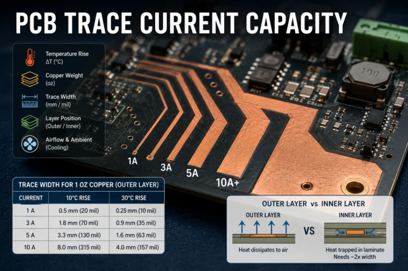
PCB Current Calculator: Sizing Trace Width and Vias with the IPC-2221 Formula
Figure 1. Pcb Current Calculator reference image for PCB...
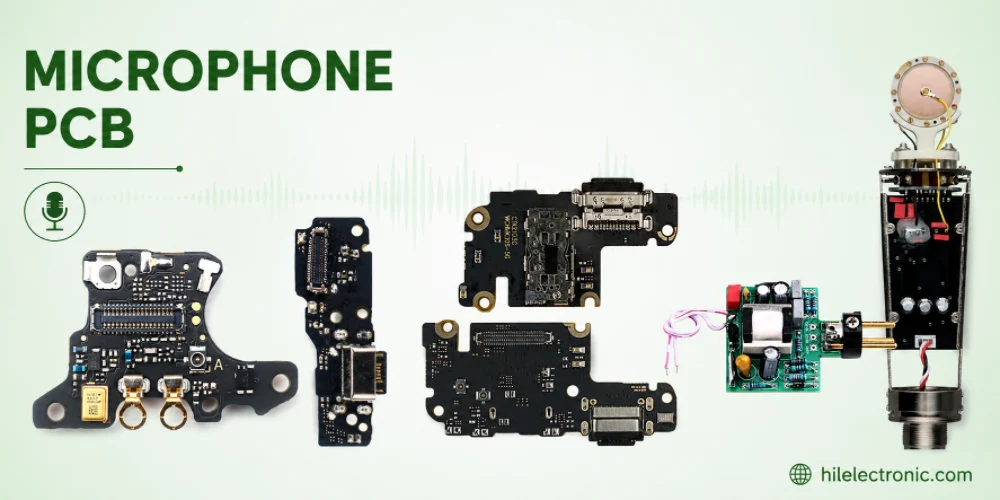
Microphone PCB Design: How the Board Itself Shapes Your Audio Quality
Figure 1. Microphone Pcb reference image for PCB...
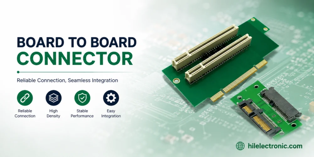
Board-to-Board Connector: Types, Specifications, and How to Select One
Figure 1. Board To Board Connector reference image for PCB...
PCB Trace Width Calculator: How to Size Traces for Current, Voltage Drop, and Impedance
Figure 1. A PCB trace width calculator is a starting point...