
Back to blog
Best Practices for Designing a PCB Layout

Introduction
A reliable PCB layout is built around manufacturability, signal integrity, power integrity, thermal behavior, and assembly access, not only around routing density. Before production, Highleap Electronics checks component placement, clearances, copper balance, impedance constraints, drill-to-copper spacing, solder mask openings, and output files so the layout can move cleanly from engineering review to fabrication; related checks are explained in PCB design for manufacturing and the Gerber file review checklist.
The sections below focus on practical PCB layout decisions that affect fabrication yield, assembly quality, testing, and repeat production, from foundational placement rules to more advanced routing and manufacturing review points.
The Crucial Role of PCB Layout
Before we dive into the depths of PCB layout best practices, it’s crucial to grasp the pivotal role that PCBs play in modern electronics. PCBs are the backbone of electronic devices, providing the structural and electrical foundation on which components are meticulously arranged. They serve as the intricate highways through which electrical signals navigate, ensuring the seamless operation of our technological marvels.
Evolution of PCBs
To appreciate the significance of PCB layout, a brief historical perspective is invaluable. In the early days of electronics, the predominant approach was characterized by point-to-point wiring and manual soldering. While functional, this method was plagued by challenges such as signal interference and reliability issues. Over time, as wires aged and insulation deteriorated, electronic failures became increasingly common.
The emergence of PCBs marked a revolutionary shift in electronic design. These boards, with their layered composition and precisely etched copper pathways, offered a reliable alternative to the web of wires. Beyond enhancing reliability, PCBs enabled miniaturization, paving the way for smaller and more efficient electronic devices.
PCBs: The Backbone of Electronics
PCBs are the lifeblood of electronic devices, providing the canvas upon which electronic components are intricately arranged and interconnected. They are the conduits through which electrical signals flow, dictating the functionality, reliability, and manufacturability of electronic products. From smartphones and laptops to medical equipment and aerospace technology, PCBs underpin the modern world of electronics.
Understanding the central role of PCB layout is paramount. It determines not only the device’s performance but also its reliability and manufacturability. A well-executed PCB layout can elevate a product to new heights, while a subpar design can lead to a cascade of issues, including electrical noise, heat dissipation problems, and production inefficiencies.
In the subsequent sections, we will embark on a comprehensive exploration of PCB layout best practices. These principles, techniques, and strategies are the building blocks of precision in PCB layout, and mastering them is essential for engineers and designers seeking to create electronics that adhere to the highest standards.

The Fundamentals of PCB Layout
A solid foundation in PCB layout begins with understanding the core principles that govern its design. In this section, we delve into the fundamental concepts that serve as the bedrock of PCB layout best practices.
Component Placement
Precision in Placement: One of the fundamental principles of PCB layout is meticulous component placement. Components should be strategically positioned to minimize signal interference, optimize signal paths, and facilitate efficient routing. High-frequency components, for instance, should be placed closer to the central processing unit (CPU) to minimize signal travel distances.
Thermal Considerations: Heat-generating components require special attention. Placing them in close proximity can lead to thermal issues and reduced reliability. Adequate spacing and heat dissipation mechanisms, such as heat sinks or thermal vias, must be incorporated into the layout.
Logical Grouping: Grouping components with related functions or signal paths can simplify routing and improve overall layout organization. This logical grouping aids in maintaining clarity and minimizing the chances of errors during the design phase.
Signal Routing
Trace Length Matching: Achieving precise signal timing is critical in high-speed electronics. Ensuring that traces carrying signals with similar propagation requirements have matching lengths helps eliminate timing discrepancies and signal skew.
Signal Integrity: Maintaining signal integrity is paramount. Techniques such as controlled impedance routing and avoiding sharp corners in traces are vital to prevent signal degradation and reflections.
Layer Stacking: Multi-layer PCBs offer greater routing flexibility. Proper layer stacking, with consideration for power and ground planes, helps reduce interference and noise, enhancing overall signal quality.
Power Distribution
Decoupling Capacitors: Placing decoupling capacitors strategically near power pins of integrated circuits (ICs) helps stabilize power distribution and suppress voltage fluctuations, ensuring consistent IC performance.
Power Plane Design: Well-designed power planes with low impedance paths are essential for efficient power distribution. They provide a stable voltage reference and minimize voltage drop, particularly in high-current applications.
Grounding Strategies: Employing proper grounding techniques, such as star grounding or split ground planes, is essential to mitigate ground loops and minimize noise.
Design for Manufacturability (DFM)
Design Rule Checking (DRC): Regularly conducting DRC checks helps identify layout errors and violations early in the design process, preventing costly manufacturing issues.
Component Libraries: Maintaining accurate component libraries with footprint information ensures precise component placement and minimizes the risk of soldering errors.
Clearance and Spacing: Adhering to recommended clearance and spacing guidelines helps avoid manufacturing defects, such as solder bridges, and ensures proper solder mask application.
EMI and EMC Considerations
Shielding and Grounding: Implementing shielding techniques and proper grounding is crucial for minimizing electromagnetic interference (EMI) and ensuring compliance with electromagnetic compatibility (EMC) standards.
Filtering: Integrating passive components like ferrite beads and EMI filters into the layout can help attenuate unwanted high-frequency noise.
Trace Routing: Paying attention to the routing of sensitive traces, such as differential pairs, and employing differential signaling techniques can reduce susceptibility to EMI.
Thermal Management
Heat Dissipation: Effective thermal management is vital for preventing component overheating. Proper placement of heat-generating components and the inclusion of thermal vias or heatsinks are common strategies.
Thermal Relief: Using thermal relief connections for components connected to copper pours aids in soldering and thermal dissipation.
Simulation: Thermal simulation tools can help predict temperature profiles within the PCB, enabling proactive design adjustments.
Comprehensive Documentation: Thorough and organized documentation, including assembly drawings, bill of materials (BOM), and fabrication files, streamlines the manufacturing and assembly processes.
Version Control: Implementing version control systems ensures that design revisions are tracked and managed effectively.
Design Iteration and Testing
Prototyping: Prototyping allows for real-world testing and validation of the PCB layout. Identifying and addressing issues early in the development process can save time and resources.
Testing and Validation: Rigorous testing, including electrical testing and signal integrity analysis, is essential to ensure that the final PCB layout meets design requirements.
Beyond the fundamentals, advanced PCB layout strategies can further elevate the precision and performance of electronic designs. Let’s explore some of these advanced techniques:
High-Speed Design Considerations
Transmission Line Theory: Understanding transmission line theory is crucial for handling high-speed signals. Impedance matching, controlled impedance, and minimizing signal reflections are vital aspects of high-speed design.
Differential Pair Routing: High-speed interfaces often rely on differential signaling to minimize electromagnetic interference and improve signal integrity. Routing differential pairs with consistent length and spacing is essential.
Clock Distribution: Proper clock distribution is critical for synchronous systems. Careful consideration of clock trace routing, skew minimization, and signal termination is necessary for reliable operation.
RF and Microwave PCBs
RF Design Fundamentals: Radio frequency (RF) and microwave PCBs have unique requirements. Understanding RF fundamentals, such as characteristic impedance and return loss, is essential for designing RF circuits.
RF Component Placement: Precise placement of RF components, such as antennas, filters, and amplifiers, is crucial to minimize signal loss and interference.
EM Modeling: Advanced tools for electromagnetic (EM) modeling and simulation help optimize RF and microwave PCB designs, ensuring optimal signal performance.
Flex and Rigid-Flex PCBs
Flex Circuit Design: Flex PCBs offer flexibility and space-saving advantages. Proper design of flex circuits involves accommodating bending and ensuring signal integrity in dynamic applications.
Rigid-Flex Integration: In rigid-flex PCBs, the integration of rigid and flexible sections demands careful planning. Ensuring smooth transitions and robust connections between sections is key.
Material Selection: Choosing the right materials for flex and rigid-flex PCBs, including substrate and coverlay materials, is critical to meeting mechanical and electrical requirements.
HDI (High-Density Interconnect) PCBs
Microvia Technology: HDI PCBs employ microvias to achieve high component density. Understanding microvia technology and its implications on signal integrity is essential.
Fine Pitch Components: Miniaturization and fine-pitch components require precise placement and routing techniques to maintain manufacturability and reliability.
Laser Drilling: Laser drilling for microvias demands expertise in laser technology and material considerations for achieving high-density interconnects.
Advanced Materials and Stackups
High-Frequency Materials: Designing for high-frequency applications requires specialized materials with low dielectric constant (Dk) and low loss tangent (Df).
Material Compatibility: Ensuring compatibility between materials in multi-layer stackups is vital to prevent delamination and maintain structural integrity.
Thermal Materials: In applications with high thermal demands, selecting thermally conductive materials and optimizing heat dissipation strategies is critical.
Conclusion
Mastering the art and science of PCB layout is a continuous journey. It demands a deep understanding of electronics, materials, signal integrity, and manufacturing processes. While this guide provides a comprehensive overview of PCB layout best practices, it’s essential to stay updated with evolving technologies and design methodologies.
In the ever-evolving landscape of electronics, precision in PCB layout remains an indispensable element in creating reliable, efficient, and innovative electronic devices. As you embark on your PCB layout endeavors, remember that attention to detail, adherence to best practices, and a commitment to continuous learning will set the stage for success in this dynamic field. Whether you’re designing a consumer gadget, a medical instrument, or a spacecraft, the PCB layout is the canvas upon which your electronic masterpiece takes shape. Embrace the art, embrace the science, and let precision be your guiding light in the world of PCB design.

Related Articles
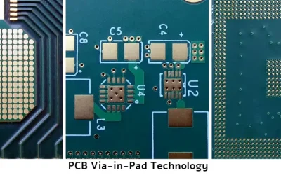
Comprehensive Analysis of PCB Via-in-Pad Technology
Explore the key advantages and challenges of Via-in-Pad technology in PCB design, with expert tips for maximizing performance and reliability.
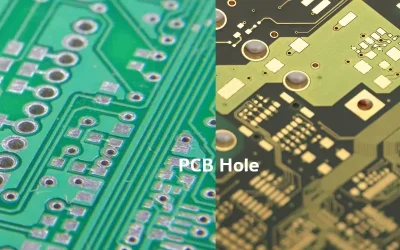
PCB Hole Selection to Optimize PCB Performance and Cost
Discover how to optimize your PCB designs with effective hole selection techniques like back drilling vs buried vias, mechanical vs laser drilling, and HDI stack planning to improve performance while minimizing manufacturing complexity and costs.
PCB Manufacturing Process Flow – Ultimate Guide Is Here
High-Quality PCB Manufacturing Solutions: Precision, Speed, and Reliability for Your Electronics Projects – From Prototype to Mass Production.
Take a Quick Quote