
Back to blog
Basics of PCB Traces: Best Practices & Techniques

PCBs are fundamental to modern electronics, providing the intricate pathways that connect components and enable electronic devices to function. Among the key elements of a PCB are traces, which are conductive paths that facilitate the flow of electrical current. This guide delves into the depths of PCB traces, covering their significance, various types, design considerations, and troubleshooting methodologies.
Understanding PCB Traces
PCB traces are the conductive pathways on a PCB that establish connections between components, allowing for the transmission of electrical signals and power throughout the circuit. Typically made of copper, these traces are etched onto the PCB substrate and are crucial for the proper functioning of electronic devices.
Importance of PCB Traces
PCB traces are essential for ensuring efficient current flow, minimal signal loss, and effective thermal management within electronic devices. Poorly designed traces can lead to signal degradation, power inefficiency, and even device failure.
Types of PCB Traces
- Signal Traces: Transmit electrical signals between components.
- Power Traces: Carry power from the source to various parts of the circuit.
- Ground Traces: Provide a path for current to return to the power source, reducing noise.
- Differential Traces: Transmit differential signals to reduce electromagnetic interference.
- Clock Traces: Transmit clock signals to synchronize components’ operations.
Design Considerations for PCB Traces
Designing PCB traces requires attention to several factors, including trace width, length, thickness, signal integrity, and thermal management. These factors ensure optimal performance and reliability of electronic devices.
PCB Trace Resistance
PCB trace resistance is a crucial consideration in the design and implementation of printed circuit boards (PCBs). It plays a significant role in determining the performance and reliability of electronic circuits, impacting factors such as signal integrity, power efficiency, and thermal management. Understanding the fundamentals of PCB trace resistance, including its calculation, factors affecting it, and the importance of managing it, is essential for electronics engineers and designers.
Calculation of PCB Trace Resistance
The resistance of a PCB trace can be calculated using Ohm’s Law, which states that resistance (R) is equal to the voltage (V) across the trace divided by the current (I) flowing through it. Mathematically, this can be expressed as:

When calculating the electrical properties of a trace on a PCB, factors such as the physical dimensions (represented by L, W, and T for length, width, and thickness respectively), the resistivity of the PCB material (represented as ΡCB), and the temperature coefficient of copper (represented as α) are taken into account. However, it’s important to note that these calculations can only provide an approximate value and the actual physical cost may vary slightly after production.
Factors Affecting PCB Trace Resistance
- Trace Length: Longer traces have higher resistance than shorter ones. This is because the resistance of a conductor is directly proportional to its length.
- Trace Width: Wider traces have lower resistance than narrower ones. The resistance of a conductor is inversely proportional to its cross-sectional area, which is determined by its width.
- Trace Thickness: Thicker copper traces have lower resistance than thinner ones. This is because the resistance of a conductor is inversely proportional to its cross-sectional area, which is determined by its thickness.
- Trace Material: The material from which the trace is made also affects its resistance. Copper is commonly used in PCB traces due to its high conductivity and low cost. Other materials, such as aluminum or gold, can be used for specific applications but may have different resistance characteristics.
Importance of Managing PCB Trace Resistance
Proper management of PCB trace resistance is crucial for several reasons:
- Signal Integrity: Excessive trace resistance can lead to signal degradation, resulting in errors or malfunctions in the circuit. By managing trace resistance, signal integrity can be maintained, ensuring reliable communication between components.
- Power Efficiency: Higher trace resistance results in higher power dissipation, leading to inefficiencies in the circuit. By keeping trace resistance low, power efficiency can be improved, reducing energy consumption and heat generation.
- Thermal Management: PCB traces with high resistance can generate heat, which can affect the performance and reliability of nearby components. By managing trace resistance, heat generation can be minimized, improving the overall thermal management of the PCB.
Overall, PCB trace resistance is a critical parameter that must be carefully managed in circuit design. By understanding the factors that affect trace resistance and the importance of managing it, designers can create reliable and efficient electronic circuits.
PCB Trace Width
Determining the ideal width for a PCB trace involves considering factors such as the expected current flow, copper thickness, and permissible temperature rise. Several tools and formulas are available to assist designers in this calculation process. By inputting parameters such as current requirements and environmental conditions, designers can accurately determine the required trace width to meet the circuit’s performance specifications.
Factors Influencing PCB Trace Width
Several factors influence the selection of PCB trace width, including:
- Current-Carrying Capacity: The width of a trace directly affects its ability to carry current without overheating. Higher current requirements necessitate wider traces to minimize resistance and prevent excessive heating.
- Copper Thickness: Thicker copper layers offer lower resistance and higher current-carrying capacity. Designers must consider the thickness of the copper layer when determining the appropriate trace width.
- Temperature Rise: Excessive current flow through a narrow trace can lead to temperature rise, potentially causing performance issues or damage to the PCB. Selecting an adequate trace width helps mitigate temperature rise and ensures reliable operation under various operating conditions.
- Signal Integrity: While wider traces offer lower resistance and better current-carrying capacity, they can also impact signal integrity by increasing parasitic capacitance and signal reflections. Designers must strike a balance between trace width and signal integrity requirements to maintain optimal circuit performance.
Importance of Proper Trace Width Selection
Properly sizing PCB trace widths is critical for preventing issues such as overheating, signal degradation, and reliability issues in electronic devices. By carefully considering factors such as current requirements, copper thickness, and signal integrity, designers can ensure that PCB traces meet performance specifications while maintaining robustness and reliability.
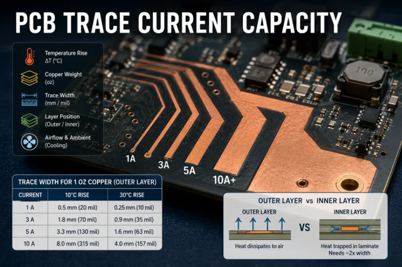
PCB Trace Current Capacity
The current-carrying capacity of a PCB trace is a fundamental parameter that directly impacts the performance and reliability of electronic circuits. Designers must accurately calculate this capacity and implement effective thermal management techniques to prevent issues such as overheating and signal degradation.
Calculating PCB Trace Current Capacity
Determining the current capacity of a PCB trace involves considering various factors, including:
- Trace Width: Wider traces offer lower resistance and can safely carry higher currents without overheating. Designers can use standardized charts or online calculators to determine the appropriate trace width based on the expected current load.
- Copper Thickness: Thicker copper layers reduce resistance and increase the current-carrying capacity of PCB traces. By selecting an adequate copper thickness based on the application’s requirements, designers can enhance the trace’s ability to handle high currents.
- Temperature Rise: Excessive current flow through a trace can lead to temperature rise, potentially causing performance issues or even damaging the PCB. Designers must consider the ambient temperature and the expected temperature rise when calculating the current capacity of a trace.
Thermal Management for PCB Traces
Proper thermal management is essential for ensuring that PCB traces can effectively dissipate heat generated by current flow. Several techniques can be employed to enhance thermal performance, including:
- Increasing Trace Width: Widening the traces reduces resistance and enhances heat dissipation, allowing the trace to carry higher currents without overheating.
- Using Thicker Copper Layers: Thicker copper layers offer lower resistance and improved thermal conductivity, enabling traces to handle higher current loads more effectively.
- Adding Thermal Vias: Thermal vias provide a path for heat to transfer from the trace to the PCB’s inner layers or to a heatsink, thereby reducing the risk of overheating and enhancing overall thermal performance.
By implementing these thermal management techniques, designers can optimize the current-carrying capacity of PCB traces and ensure the reliability and longevity of electronic circuits.
Overall, accurately calculating the current capacity of PCB traces and implementing effective thermal management strategies are essential steps in designing robust and reliable electronic systems. By considering factors such as trace width, copper thickness, and temperature rise, designers can optimize the performance of PCB traces and mitigate the risk of overheating and signal degradation.
Repairing and Troubleshooting PCB Traces
Despite meticulous design and manufacturing processes, PCB traces may encounter issues ranging from mechanical stress to manufacturing defects. Repairing and troubleshooting these traces demand meticulous attention and strategic interventions to ensure optimal circuit functionality.
Repair Techniques for PCB Traces
- Jumper Wires: When a trace is damaged or severed, jumper wires serve as a practical solution to bridge the gap, restoring electrical continuity. Careful soldering techniques and proper insulation are essential to prevent unintended short circuits or signal interference.
- Conductive Ink: Conductive ink offers a versatile option for repairing minor trace damage or creating new connections. Applied with precision, conductive ink forms a reliable electrical pathway, particularly suitable for delicate circuitry or intricate designs.
- Wire Wrapping: In cases where traditional soldering methods may not be feasible, wire wrapping provides an alternative approach. By securely wrapping fine-gauge wire around component leads or connection points, technicians can establish robust electrical connections without the need for solder.
Troubleshooting Strategies for PCB Traces
- Diagnostic Tools: Multimeters and oscilloscopes are indispensable tools for diagnosing PCB trace issues. Multimeters enable precise measurement of resistance, continuity, and voltage, aiding in the identification of open circuits or high-resistance traces. Oscilloscopes offer real-time visualization of signal waveforms, facilitating the detection of abnormalities such as noise or distortion.
- Visual Inspection: A thorough visual inspection of the PCB surface can reveal visible signs of damage or defects, such as cracks, burns, or solder splashes. Magnification tools and proper lighting enhance the accuracy of the inspection process, allowing technicians to pinpoint areas requiring attention.
- Component Testing: In cases where trace issues are suspected to originate from component failure, individual components can be tested using specialized equipment or substitution methods. By systematically isolating and testing components, technicians can identify faulty elements contributing to trace-related issues.
By leveraging a combination of repair techniques and troubleshooting strategies, technicians can effectively address PCB trace issues, restoring circuit functionality and mitigating potential downtime. Adopting a systematic approach to repair and troubleshooting ensures thoroughness and accuracy in identifying and rectifying trace-related issues, ultimately enhancing the reliability and performance of electronic systems.
Conclusion
Overall, PCB traces play a crucial role in ensuring the functionality and reliability of electronic devices. It is essential for electronics designers and manufacturers to have a comprehensive understanding of the design considerations, calculation methods, and troubleshooting techniques related to PCB traces.
By adhering to the guidelines outlined in this guide, designers can create PCBs that meet performance specifications and operate reliably in their intended applications. Proper management of trace resistance, width, and current capacity is vital for maintaining signal integrity, preventing overheating, and ensuring the longevity of electronic devices.
Additionally, employing effective repair and troubleshooting strategies can help address trace-related issues that may arise during the lifespan of a PCB. By staying informed and implementing best practices, electronics professionals can optimize the performance and reliability of PCBs, contributing to the advancement of electronic technologies.
For production planning, it also helps to compare this topic with electronic component sourcing and Rogers laminate PCB fabrication before finalizing the fabrication or assembly package.

Recommended Posts

PCB Current Calculator: Sizing Trace Width and Vias with the IPC-2221 Formula
Figure 1. Pcb Current Calculator reference image for PCB...

Microphone PCB Design: How the Board Itself Shapes Your Audio Quality
Figure 1. Microphone Pcb reference image for PCB...

Board-to-Board Connector: Types, Specifications, and How to Select One
Figure 1. Board To Board Connector reference image for PCB...
PCB Trace Width Calculator: How to Size Traces for Current, Voltage Drop, and Impedance
Figure 1. A PCB trace width calculator is a starting point...