
PCB Trace Design Guide: Width, Routing, and Repair

PCB Trace Design Guide for Reliable Board Performance
PCB traces are the conductive paths that connect components on a printed circuit board and carry signals, power, and data throughout the circuit. Their design has a direct impact on signal integrity, thermal performance, manufacturability, and long-term product reliability. While many designers begin with the basic structure and function of PCB traces, successful layouts require a deeper understanding of routing strategy, copper thickness, reference planes, and current capacity.
In modern electronics, trace design is no longer just about drawing copper between pads. It is a key part of overall PCB engineering, especially in high-speed, high-current, and dense multilayer applications. Designers must consider how trace width, spacing, copper weight, and layer arrangement work together to support stable electrical performance.
Why PCB Trace Design Matters
Poorly designed traces can lead to voltage drop, overheating, EMI issues, and signal distortion. By contrast, well-routed traces improve electrical stability and make the board easier to manufacture and assemble. In many multilayer designs, trace behavior is also closely tied to PCB stackup planning, because layer configuration affects impedance, return path continuity, crosstalk control, and thermal distribution.
For this reason, trace design should always be evaluated in the context of the complete board, not as an isolated layout task. Even small routing choices can influence the final performance of high-density or high-frequency PCBs.
PCB Trace Thickness and Current Capacity
Trace thickness, typically defined by copper weight, plays an important role in current-carrying ability and heat dissipation. Thicker copper allows traces to handle larger currents with lower resistive heating, which is critical in power electronics, motor control, and industrial systems. In applications that demand especially high current handling, designers often refer to heavy copper PCB current capacity considerations to determine whether standard copper is sufficient or if a more robust structure is required.
Thinner traces may support compact routing and higher pin-density layouts, but they also reduce electrical and thermal margin. The right balance depends on the application, available board area, allowable temperature rise, and production capability.
How to Determine PCB Trace Width
Trace width is usually calculated based on recognized industry standards and then refined according to actual design conditions. The two most referenced methods are IPC-2221 and IPC-2152.
IPC-2221
IPC-2221 is the traditional formula-based approach used to estimate how much current a trace can carry under a specified temperature rise. It remains useful as a general reference, but it does not fully reflect the thermal realities of modern PCB structures.
IPC-2152
IPC-2152 provides a more accurate framework because it incorporates additional factors such as board construction, copper thickness, and heat dissipation environment. For designs where routing must also satisfy controlled signal behavior, trace geometry is often reviewed together with controlled impedance PCB requirements to ensure that width selection supports both current handling and transmission performance.
In practical design work, engineers typically start with a calculator or CAD-based rule set, then adjust width values based on copper distribution, airflow, layer location, and fabrication tolerances.
Best Practices for PCB Trace Routing
1. Route Critical Nets with Purpose
Autorouting can save time, but sensitive nets should still be routed intentionally. Clocks, differential pairs, RF lines, and analog signals often benefit from manual routing because they require tighter control over length, spacing, and return path quality.
2. Match Trace Width to Electrical Function
Power traces, signal traces, and impedance-controlled traces do not follow the same design rules. Width should always be selected according to electrical function rather than available space alone. Extremely narrow conductors may simplify dense layouts, but they can increase resistance, heat buildup, and manufacturing difficulty.
3. Preserve a Continuous Return Path
Signal traces perform best when routed over a solid reference plane. A stable ground plane reduces loop area, improves return current behavior, and lowers noise sensitivity. This is especially important in high-speed digital designs where trace routing and layer transitions strongly affect EMI performance.
4. Reduce Coupling and Crosstalk
Adjacent traces can interfere with one another through capacitive and inductive coupling. Greater spacing between sensitive nets helps reduce unwanted interaction. Designers should also separate analog, digital, and switching power sections whenever possible.
5. Pay Attention to Vias in the Signal Path
Trace routing is not only about horizontal copper paths. Every via introduces discontinuity, parasitic effects, and manufacturing considerations. When signals transition between layers, it is important to understand how different blind and buried via structures may influence routing density, signal quality, and layer utilization in advanced PCB layouts.
6. Coordinate Trace Design with High-Speed Requirements
As edge rates increase, trace behavior becomes more dependent on stackup symmetry, reference plane quality, and impedance consistency. In these cases, routing decisions should be reviewed together with high-speed PCB stackup design strategies so that the board can support reliable transmission without excessive reflection, skew, or radiated noise.
Common Causes of PCB Trace Problems
Trace failures may result from excessive current, overheating, corrosion, poor fabrication quality, rework damage, or mechanical stress. Some failures are obvious, such as open circuits or burned copper, while others appear as intermittent faults, unstable signals, or unexpected noise.
Before repairing a damaged trace, it is important to identify the root cause. If the original failure was caused by thermal overload or poor current distribution, simply reconnecting the copper path may not prevent the same issue from happening again.
How to Repair a Damaged PCB Trace
PCB trace repair is often used for prototypes, test boards, maintenance work, or low-volume electronics. A typical repair process includes the following steps:
- Locate the damaged section of the trace.
- Remove the broken or burnt portion carefully without damaging nearby pads or components.
- Clean the exposed copper surface thoroughly.
- Apply flux and tin the exposed ends.
- Select a suitable replacement wire with the correct gauge.
- Strip and tin both ends of the wire if needed.
- Solder the first end securely with enough overlap onto the original copper.
- Route and secure the wire neatly along the board surface.
- Solder the second end and verify continuity.
- Clean away any remaining flux residue and inspect the repaired area.
For high-frequency or fine-pitch boards, repair should be approached carefully because even minor geometry changes can affect electrical behavior.
Conclusion
PCB trace design influences nearly every aspect of circuit board performance, from current delivery and thermal stability to signal integrity and manufacturability. A reliable layout depends on choosing the right trace width, maintaining proper spacing, controlling return paths, and coordinating routing with the overall board structure.
Designers who already understand the fundamentals of PCB traces can improve board quality significantly by focusing on routing discipline, stackup planning, and application-specific electrical requirements. When these elements are handled correctly, PCB manufacturing becomes more predictable, and the finished product performs more consistently in real-world conditions.

Related Articles

Underwater & Pool LED Light PCBs: IP68 Potted Boards, Low-Voltage Drivers & Safety
Manufacture LED pool light PCBs for IP68 potted underwater fixtures, low-voltage drivers, RGBW boards and corrosion-resistant assemblies.
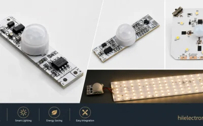
Motion Sensor & Smart LED Light PCBs: Sensor, Control, Driver & Wireless Boards
Build motion sensor LED light PCBs with PIR or microwave sensing, MCU control, wireless modules, drivers and smart-lighting PCBA integration.

LED High Bay Light PCBs: Metal-Core Light Engines, Drivers & Turnkey Boards Built to Spec
Get LED high bay light PCB fabrication and assembly for metal-core engines, drivers, surge boards, sensors and industrial lighting programs.