
Back to blog
Signal reflections and distortion in Printed Circuit Boards

Signal reflections and distortion
As electronic devices become increasingly complex and operate at higher speeds, the challenges of maintaining pristine signal quality intensify. Among these challenges, signal reflection and distortion stand as formidable foes, threatening to undermine the very foundation of electronic communication. In this comprehensive guide, we delve into the intricacies of signal reflection and distortion, unraveling their causes, effects, and offering strategic solutions to combat them effectively.
What is Signal Reflection?
Signal reflection occurs when a signal encounters an impedance mismatch or discontinuity within its transmission path. As the signal travels through mediums such as cables, antennas, or PCB traces, it encounters changes in impedance, causing a portion of the signal to bounce back toward its source. This phenomenon leads to signal loss, interference, and degradation, posing a significant challenge in high-speed and high-density PCB designs.
Unveiling the Causes of Signal Reflection
Signal reflection arises from a variety of factors within communication systems. Changes in the impedance of transmission lines due to cable type variations, connectors, or improperly terminated cables can contribute to this issue. Signals traversing mediums with varying dielectric constants or improper termination devices can also experience reflections. Additionally, faulty or damaged equipment, as well as cable lengths that are not multiples of the wavelength, can exacerbate signal reflection.
The Ripple Effects of Signal Reflection
The consequences of signal reflection on PCB performance are far-reaching and detrimental. Signal integrity degradation, increased crosstalk, heightened electromagnetic interference (EMI), and timing issues are just a few of the adverse effects. As signal frequencies increase and timing margins tighten, even minor reflections can lead to communication errors, bit errors, and erroneous data interpretations, ultimately compromising the reliability and performance of the PCB.

Mitigating Signal Reflection: Strategies for Success
Impedance Matching
Ensuring proper impedance matching between the signal source, transmission line, and load is crucial for reducing signal reflection. Techniques such as series, parallel, Thevenin, or AC termination can be employed to achieve optimal impedance matching, minimizing the impedance discontinuities that give rise to reflections.
Designing controlled impedance transmission lines, such as microstrip or stripline, is essential for maintaining consistent impedance throughout the PCB. Carefully selecting the appropriate trace width, dielectric material, and thickness can help achieve this goal, thereby reducing the likelihood of signal reflections.
Signal Routing and Layer Stack-up
Implementing proper signal routing techniques is vital for minimizing impedance discontinuities and reflections. Shorter trace lengths, avoiding sharp corners, and maintaining consistent trace widths all contribute to a smoother signal propagation. Additionally, optimizing the layer stack-up design can balance signal integrity, EMI, and manufacturing costs, further enhancing overall performance.
Differential Signaling
Differential signaling, which utilizes two complementary signals to transmit data, offers a powerful solution for minimizing the impact of signal reflection. By leveraging the cancellation of common-mode noise and reflections, differential signaling can significantly improve signal integrity and overall system performance.
The Enigma of Signal Distortion
What is Signal Distortion?
Signal distortion refers to any undesired alteration in an electrical signal’s shape, amplitude, phase, or timing as it propagates through a medium or circuit. This phenomenon can lead to degraded performance, increased bit error rates, and communication errors, posing a significant challenge in high-speed digital and high-frequency analog circuits.
Unraveling the Causes of Signal Distortion
Signal distortion can arise from a myriad of factors within an electronic system. Impedance mismatches between the source, transmission line, and load can cause signal reflections, resulting in distortion. Non-linear components, such as diodes and transistors, can introduce harmonics and undesired frequency components, leading to signal distortion. Additionally, parasitic elements like capacitance, inductance, and resistance in PCB traces, connectors, and components can contribute to phase and amplitude distortion, while crosstalk from adjacent signal lines can cause interference and further distortion.
The Ripple Effects of Signal Distortion
The impact of signal distortion on PCB performance is multifaceted and far-reaching. Degraded signal integrity, increased crosstalk, timing problems, and higher power consumption are just a few of the consequences. As signals become distorted, issues such as ringing, overshooting, and undershooting can arise, leading to misinterpretation of signals, increased error rates, and diminished system performance. Furthermore, distortion can cause synchronization issues and corrupt data, reducing the reliability of high-speed digital systems.

Mitigating Signal Distortion: Techniques for Pristine Signal Quality
PCB Layout Design
Proper PCB layout design is a critical factor in mitigating signal distortion. Separating analog and digital signal traces to avoid crosstalk, placing high-speed signal traces away from noisy components, using shorter trace lengths to reduce signal attenuation and propagation delay, and routing differential signal pairs with consistent length and proximity are all essential strategies for maintaining signal integrity.
Impedance Control
Designing PCB traces with controlled impedance is paramount for minimizing signal reflections and distortion. Matching the impedance of the driver, transmission line, and receiver ensures seamless signal propagation, reducing the impact of impedance mismatches and discontinuities.
Grounding and Power Distribution
Implementing a solid ground plane provides a low-impedance return path and reduces EMI, while proper power distribution, achieved through multiple power and ground layers and decoupling capacitors near integrated circuits (ICs), minimizes voltage fluctuations and enhances signal quality.
Shielding and Filtering
Shielding techniques, such as enclosing sensitive components in a Faraday cage, can protect them from external EMI, while implementing low-pass filters can attenuate high-frequency noise, further enhancing signal integrity.
Differential Signaling
As previously mentioned, differential signaling offers a powerful solution for improving signal quality by canceling out common-mode noise and reflections. This technique is particularly effective in high-speed communication systems, where signal integrity is paramount.
Design Considerations for Signal Integrity
Optimizing Stack-up Design
Optimizing the layer stack-up design is crucial for maintaining signal integrity in PCBs. Placing power and ground planes adjacent to each other reduces loop inductance and provides excellent decoupling. Balancing signal integrity, electromagnetic interference (EMI), and manufacturing costs is essential for achieving optimal performance.
Impedance Control
Calculating the characteristic impedance of transmission lines based on trace geometry and dielectric properties is critical for impedance control. Matching the impedance of the driver, transmission line, and receiver is paramount for minimizing signal reflections and ensuring seamless signal propagation.
Trace Routing Techniques
Routing high-speed signals using microstrip or stripline transmission lines, maintaining consistent trace widths, avoiding sharp corners to reduce impedance discontinuities, and keeping high-speed traces as short as possible are all essential techniques for minimizing signal attenuation, delay, and distortion.
Differential Signaling Importance
Differential signaling is crucial for signal integrity. Routing differential pairs with the same length and proximity optimizes their performance, enhancing signal integrity and reducing the impact of noise and interference.
Crosstalk Minimization Strategies
Separating analog and digital signals, maintaining sufficient spacing between parallel traces, utilizing ground planes and guard traces, and implementing other crosstalk minimization strategies are vital for reducing interference and ensuring signal integrity.
Grounding and Power Distribution
Implementing a solid ground plane for a low-impedance return path and EMI reduction, along with proper power distribution through multiple power and ground layers and decoupling capacitors near ICs, is crucial for maintaining stable voltage levels and minimizing noise-induced distortion.
By carefully considering these design aspects, engineers can enhance signal integrity, reduce EMI, and optimize the performance of their PCB designs.

Signal Integrity Analysis and Simulation Tools
Popular Software for Signal Integrity Analysis
Several powerful software tools are available to aid in signal integrity analysis and simulation, ensuring optimal PCB performance. SPICE (Simulation Program with Integrated Circuit Emphasis) is a widely used circuit simulation tool for analyzing electrical performance, including signal integrity in both time and frequency domains. HyperLynx, a comprehensive suite of tools, offers pre-and post-layout simulation and optimization capabilities for signal integrity, power integrity, and EMC analysis. Additionally, Keysight ADS (Advanced Design System) is a high-frequency, high-speed design and simulation software that enables the analysis of signal integrity, power integrity, and other performance parameters in complex PCB designs.
Incorporating Simulation Results into the Design Process
To achieve optimal signal integrity, it is essential to incorporate simulation results into the design process from the outset. Running simulations early in the design phase can identify potential signal integrity issues and facilitate the optimization of trace routing, impedance matching, and termination strategies. Iterative simulations should be conducted as the design evolves, incorporating feedback and changes to address identified concerns. Additionally, evaluating different design alternatives and trade-offs, such as the impact of using alternative materials, layer stack-ups, or routing strategies on signal integrity, can provide valuable insights for informed decision-making.
Validation and Testing of the Final PCB Design
Once the PCB has been fabricated, it is crucial to perform functional testing and signal integrity measurements using appropriate tools. Comparing the measured results with simulation predictions allows for the validation of simulation accuracy and the effectiveness of the design optimizations. If discrepancies arise between simulation and measurement results, iterative design revisions and repeated validation processes may be necessary until the desired signal integrity performance is achieved.
Conclusion
In the ever-evolving landscape of electronic devices, maintaining signal integrity is paramount for ensuring reliable and efficient performance. Signal reflection and distortion, two formidable foes in this realm, can have far-reaching consequences if left unchecked. By employing strategic techniques such as impedance matching, controlled impedance lines, optimized signal routing, differential signaling, and comprehensive shielding and filtering strategies, these challenges can be mitigated effectively.
Moreover, leveraging powerful signal integrity analysis and simulation tools, incorporating simulation results into the design process, and validating the final PCB design through rigorous testing are essential steps in achieving optimal signal quality. Collaboration with experienced EMS solutions providers and a deep understanding of signal integrity principles can further enhance the success of PCB designs, ensuring that they meet the stringent demands of modern electronic systems.
Remember, the pursuit of signal integrity is an ongoing journey, one that requires unwavering dedication and a commitment to continuous improvement. By embracing the strategies outlined in this comprehensive guide and staying abreast of the latest advancements in the field, you can confidently navigate the complexities of signal reflection and distortion, ensuring that your PCB designs consistently deliver exceptional performance and reliability.
PCB & PCBA Quick Quote
Related Articles
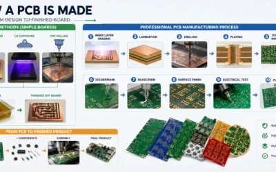
How a PCB Is Made: Fabrication Process Guide
See how a PCB is made, from home etching to professional fabrication, and learn when to move to factory processes for accuracy, yield, and assembly.
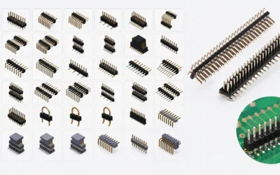
PCB Pin Headers: Selection and Mounting Guide
Learn how to choose PCB pin headers by pitch, current rating, plating, and mounting style for dependable board-to-board and cable connections.
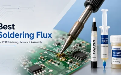
Best Soldering Flux for Electronics
Choose the best soldering flux for electronics by comparing no-clean, rosin, and water-soluble options for hand soldering, rework, and PCB assembly.