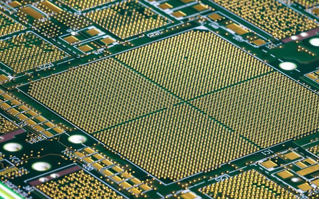
HDI Interconnect Technologies

Page 4 · Return to the topic overview

More articles

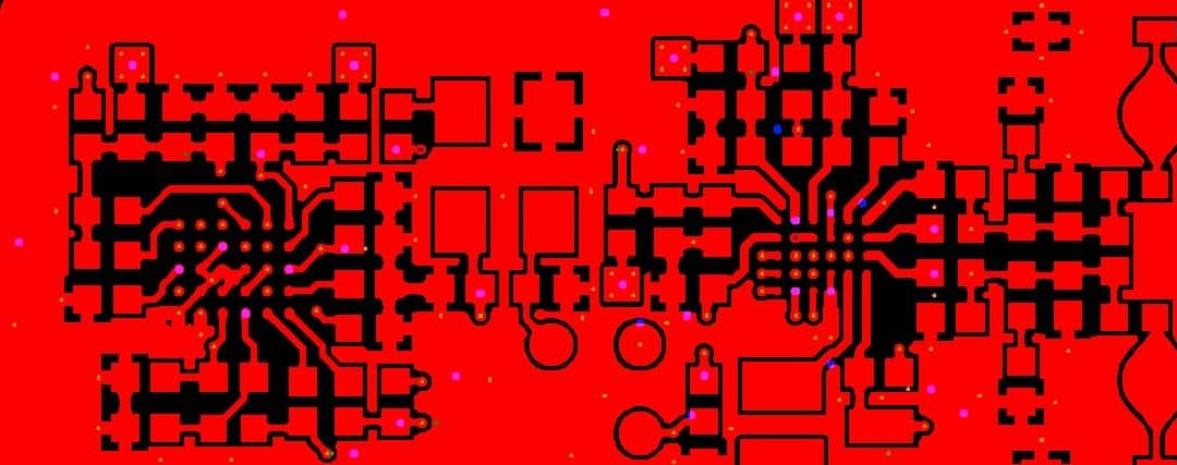
HDI PCB CAM Workflow | Define SMD, Vias, and Drill Rules

HDI PCB CAM Workflow | Define SMD, Vias, and Drill Rules

HDI PCB CAM production is one of the most technically demanding areas in PCB manufacturing. With increasing IC integration and high-density assembly requirements, HDI mobile boards often feature complex outlines, dense routing, and tight via arrangements. These...
How Blind Via PCBs Impact Electronics Manufacturing

How Blind Via PCBs Impact Electronics Manufacturing

[pac_divi_table_of_contents title="On this article" default_state="closed" included_headings="off|on|off|off|off|off" exclude_headings_by_class="on" active_link_highlight="on" level_markers_3="icons" title_container_padding="10px|15px|10px|15px|true|false"...

Application of High Density Interconnect PCB in High-Tech

Application of High Density Interconnect PCB in High-Tech

What is HDI PCB? HDI PCBs (High-Density Interconnect PCBs) are a type of printed circuit board that offer higher wiring density per unit area compared to traditional circuit boards. They are designed to meet the demands of smaller and faster electronic products. HDI...